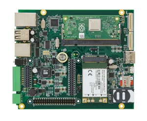
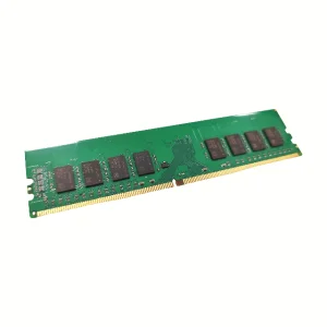
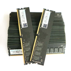
Deploying tier-one semiconductor processes and precision manufacturing systems to deliver high-performance hardware, PCBA, and integrated wireless power systems worldwide.
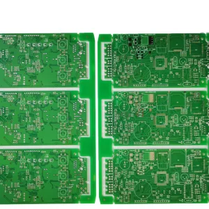
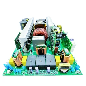
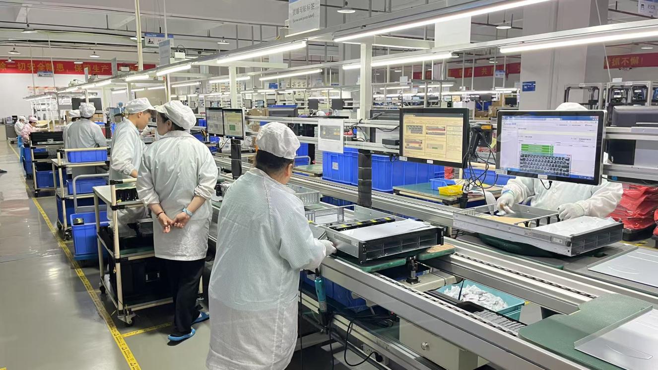
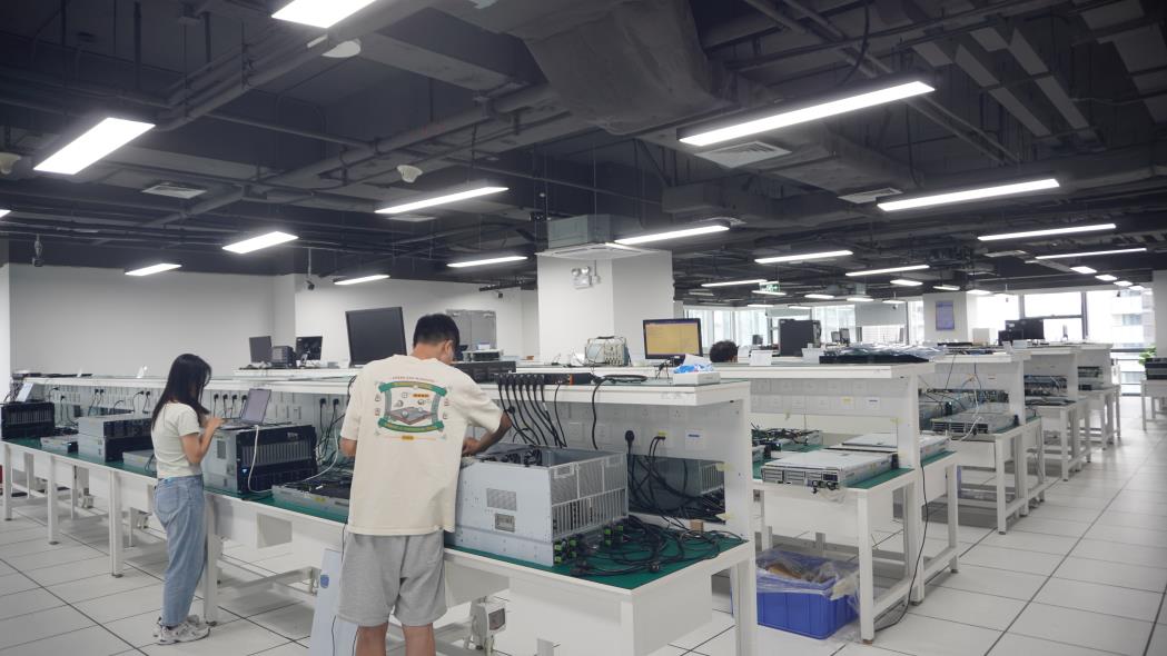
Established in 2017, Celtrix Memory Technologies Co., Ltd. has grown to become a benchmark manufacturer of advanced hardware modules, high-frequency PCB assemblies, and integrated wireless charging technologies. With a state-of-the-art facility spanning 28,600 m², we integrate full-lifecycle SMT production, automated optics inspection, and precision calibration setups to serve clients across 50+ countries.
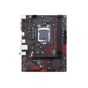
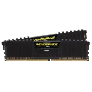
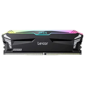
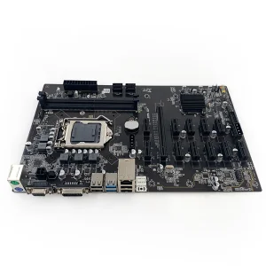
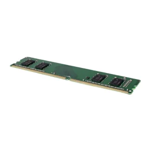
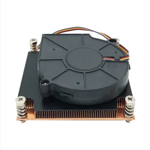
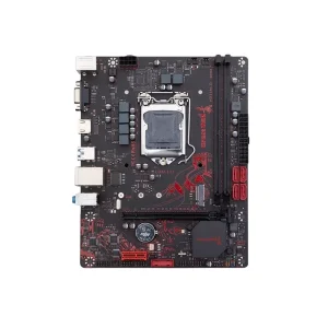
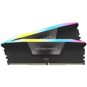
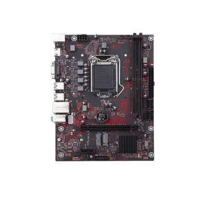
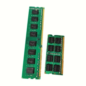
While our core legacy thrives in high-speed DDR5 memory, gaming DRAM, and complex industrial computer motherboards, our technological cross-over into high-efficiency wireless charging solutions is driven by our foundational SMT expertise, robust heat sink integrations, and complex multi-layer PCB design capabilities. Today, we stand as a premier partner for OEMs, ODMs, global distributors, and system integrators seeking high-yield, reliable wireless power transmission systems.
Analyzing the paradigm shift in electromagnetic induction, the Qi2 standard, and the surging industrial demand for cable-free power distribution.
The global commercial market is rapidly transitioning towards the WPC Qi2 standard. Implementing Magnetic Power Profile (MPP) ensures precise coil alignment, drastically minimizing eddy current heat loss and accelerating charging speeds from 7.5W to 15W and beyond.
Beyond consumer devices, factories and warehouses are adopting wireless charging for Automated Guided Vehicles (AGVs) and autonomous mobile robots (AMRs). Eliminating exposed physical pins removes spark hazards in dust-heavy industrial environments.
Urban centers are embedding wireless transmitters directly into public furniture, automotive consoles, and transit hubs. This ubiquitous mesh of low-maintenance wireless power infrastructure requires ruggedized, weather-sealed internal PCBA modules.
From a macro perspective, the global wireless charging market is projected to expand at a compound annual growth rate (CAGR) exceeding 20% over the next decade. As countries implement stricter sustainability frameworks, reducing electronic waste by standardizing charger architectures has become a legislative priority. Inductive and resonant wireless charging systems mitigate mechanical port wear, dramatically extending the operating life cycle of smart hardware.
How Celtrix translates advanced memory PCBA manufacturing precision into zero-defect electromagnetic induction charging systems.
Designing a high-yield wireless charging system requires deep expertise in electromagnetic compatibility (EMC), thermal dynamics, and high-frequency circuit layouts. At Celtrix, we leverage our 9 years of high-speed motherboard and DRAM module fabrication to engineer superior wireless charging PCBAs:
High-wattage wireless charging (such as 15W, 30W, and 50W fast-charging protocols) generates localized thermal loads on the transmitter board. Using OEM 2-layer and 4-layer lead-free HASL boards, our engineers optimize layout design using dedicated thermal vias. These vias draw heat away from the central Power Management Integrated Circuit (PMIC) and spread it across internal copper planes, keeping operational temperatures below 40°C.
To maximize coupling efficiency, we utilize custom-engineered Litz-wire coils with high Quality (Q) factors. Combined with high-permeability ferrite sheets, the magnetic flux is tightly directed toward the receiver coil, preventing electromagnetic interference (EMI) from disrupting nearby host circuits (such as DDR5 data channels or desktop computer bus lanes).
Every premium wireless charger from our factory includes an integrated MCU programmed with proprietary firmware. This chip regulates dynamic power negotiation, tracking frequency adjustments between 110kHz and 205kHz, and executing instant power cutoffs when foreign metals are detected via our advanced Foreign Object Detection (FOD) algorithms.
Ensuring global regulatory adherence and faultless operations through strict ISO-compliant inspection protocols.
With a dedicated quality control team of 56 certified professionals, we enforce rigorous inspection checkpoints at every turn:
Exporting to over 50 countries requires strict compliance with international standards. Our manufacturing processes conform to:
Tailoring electronic architectures and physical designs to match regional consumer preferences and industrial specs.
Celtrix's massive USD 23 Million annual export scale is built on flexible, customer-centric customization options. Because we control the SMT production lines and assembly lines, we offer deep-level modifications that traditional trading companies cannot provide:
We design bespoke aluminum, copper, or graphite heat spreaders to fit slim, high-end charging docks and prevent device throttling.
Modifying controllers and firmware structures to optimize power negotiation curves based on client device requirements.
Offering high-end private label branding, custom enclosure molds, and sustainable, localized packaging designs.
What lies ahead in the next generation of wireless power transfer (WPT) technologies.
As we look to the future, wireless power is evolving beyond short-range inductive coupling. Celtrix's R&D department (comprising 142 engineers) is currently tracking and prototyping several next-generation concepts:
Unlike standard inductive chargers that require surface-to-surface alignment, magnetic resonance enables spatial freedom. Devices can charge at distances of several centimeters, allowing transmitters to be mounted under thick wooden tables, stone countertops, or within industrial enclosures without drilling holes.
By using GaN semiconductors in the transmitter driver stages, we can decrease switching losses, improve energy conversion efficiency to over 90%, and halve the size of the control board. This advancement facilitates extremely compact, multi-coil desktop charger matrices.
Future charging mats will feature dynamic, beam-forming transmitter matrices capable of tracking and charging multiple receivers simultaneously at optimized power levels, eliminating the restriction of single-device charging zones.
Direct answers regarding manufacturing capabilities, pricing structure, lead times, and technical support.


 Celtrix Memory