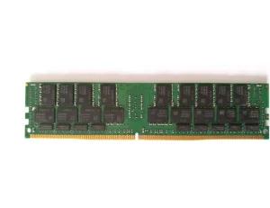
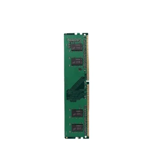
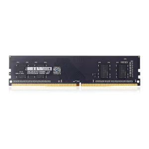
Explore our high-performance memory modules and PCB assemblies engineered to interface seamlessly with precise laser-cut solder profiles.
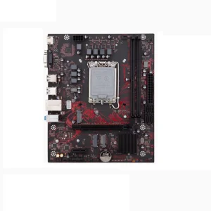
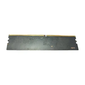
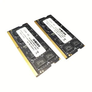
Analyzing the critical intersection of laser-cutting stencils and electronic assembly yields in high-frequency hardware applications.
In the modern SMT (Surface Mount Technology) landscape, the density of electronic assemblies has reached unprecedented levels. The introduction of high-speed memory modules, such as DDR5 and enterprise-grade servers, demands sub-micron assembly tolerances. Within this context, the SMT stencil is no longer a simple tooling commodity; it is a high-precision instrument that dictates assembly yield, solder paste transfer efficiency, and overall electrical reliability.
As a leading Custom OEM Laser Cutting Stencils Manufacturer & Exporter, our engineering philosophy revolves around solving the physical limits of solder paste release. Through the utilization of fiber laser systems operating at high frequencies with custom spot shapes, we reduce inner aperture wall roughness (Ra) to less than 0.5 μm. This whitepaper analyzes our manufacturing processes, global supply chain, and technological roadmap for micro-aperture printing solutions.
We utilize cutting-edge fiber lasers to create apertures with a kerf angle taper of 1° to 2°, facilitating rapid paste release during the separation stroke.
Advanced post-processing techniques eliminate microscopic burrs and apply a hydrophobic/oleophobic layer to reduce stencil cleaning cycles.
Frame-mounted stencils feature controlled pneumatic stretch limits to ensure stable registration across large production runs.
Leveraging massive manufacturing infrastructure to supply global high-tech industries.
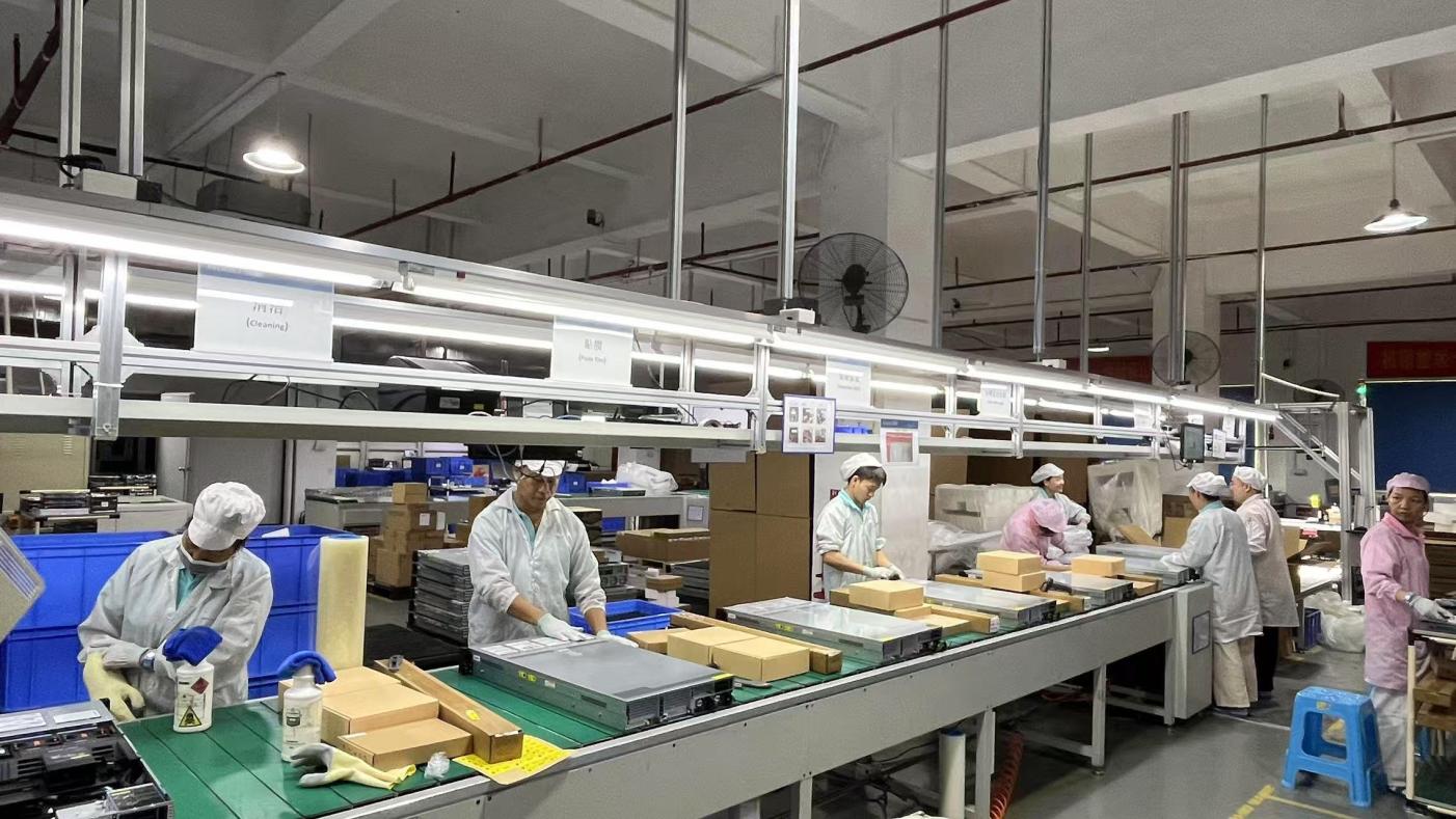
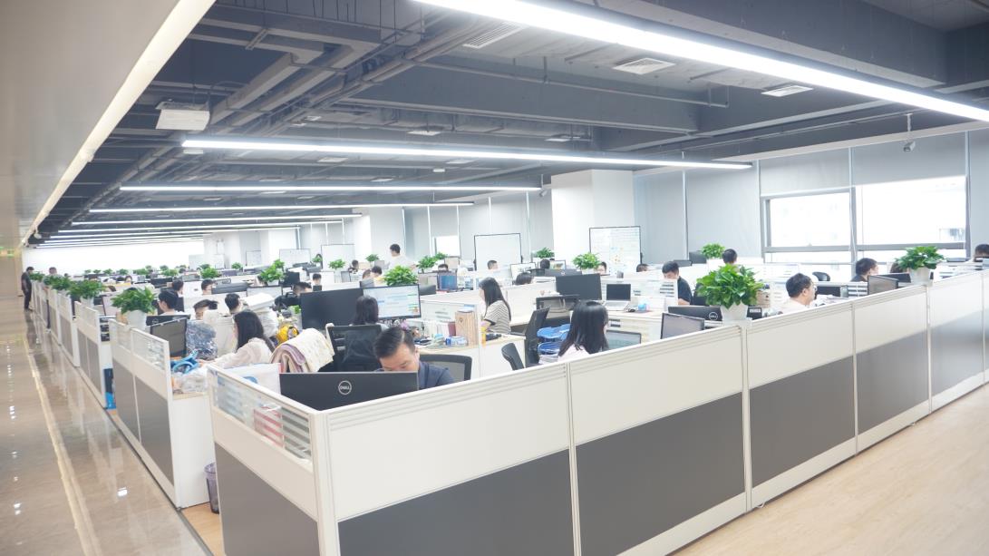
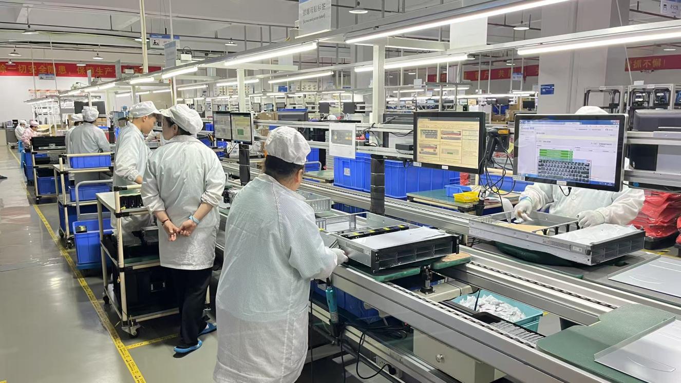
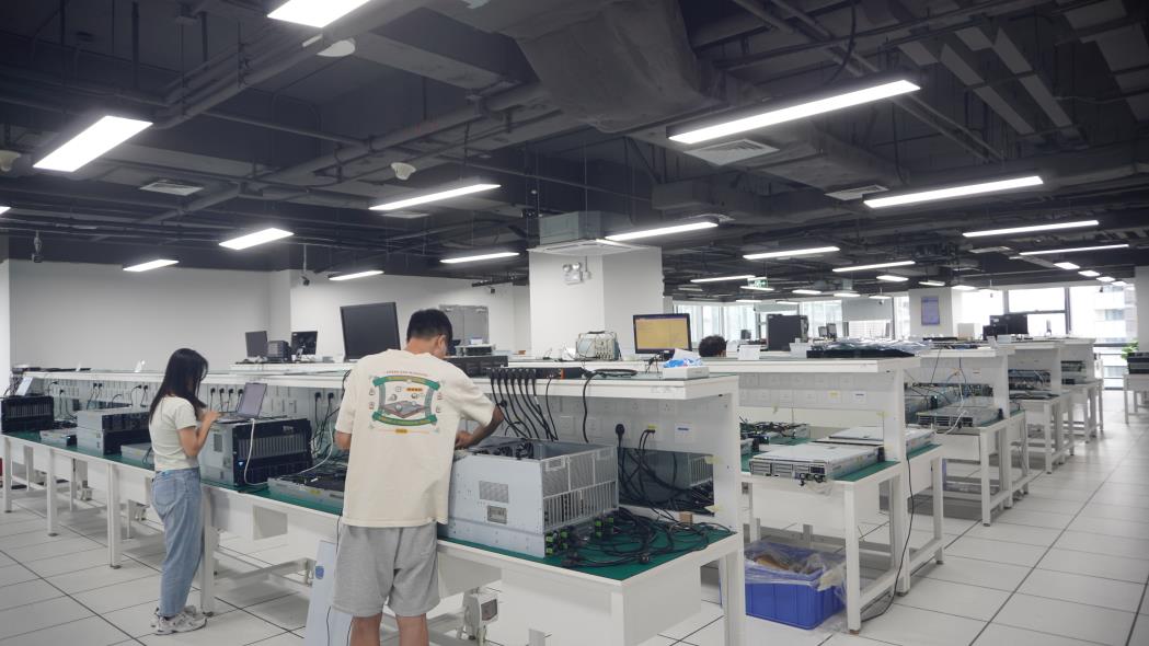
Celtrix Memory Technologies Co., Ltd., founded in 2017, is a premium manufacturer specializing in DRAM storage systems, high-density PCBs, and high-precision laser-cut stencils. Spanning a modern production area of 28,600 m², our factory is equipped with advanced SMT automated production lines and high-grade fiber laser engraving facilities.
With 9 years of industry experience and 7 years of export history, we have developed a network of over 1,180 supply chain partners, exporting high-value equipment to more than 50 countries, and generating an annual export revenue exceeding USD 23 million.
Standard design envelopes and engineering tolerances for custom SMT stencils.
Every laser-cut stencil fabricated by Celtrix is subjected to a strict design review process. Engineers analyze CAD/Gerber file architectures to optimize aperture area ratios according to the formula:
Where L is length, W is width, and T is stencil thickness. In fine-pitch printing (components under 0.4mm pitch), area ratios down to 0.50 are achieved via specialized nano-coatings.
| Parameters | Standard Specification | Fine-Pitch Optimization | Extreme Capabilities |
|---|---|---|---|
| Material Grade | Fine-Grain SUS304 / SUS301 | FG (Fine-Grain) Steel Sheet | Electroformed Nickel (Ni) |
| Thickness Tolerance | ± 5.0% | ± 3.0% | ± 1.5 μm |
| Aperture Tolerance | ± 5.0 μm | ± 3.0 μm | ± 1.5 μm |
| Positional Accuracy | ± 10 μm / 600mm | ± 8 μm / 600mm | ± 5 μm / 600mm |
| Aspect Ratio Rule | > 1.5 | > 1.2 | > 1.0 |
| Maximum Sheet Dimensions | 736 mm x 736 mm | 800 mm x 1000 mm | 1200 mm x 1500 mm |
Addressing the complex technical demands of localized assembly lines across key global hubs.
From advanced automotive driver assistance systems (ADAS) in Europe to high-frequency communication servers in North America, electronic assemblies rely on consistent stencil performance. We provide customized solutions designed to address specific industrial scenarios:
In safety-critical automotive systems (such as power management, ABS modules, and inverter PCBs), the stencil must guarantee zero solder voiding and zero bridging. Our custom stepped-up stencils allow localized increases in paste volume for high-power connectors, while stepped-down apertures limit paste deposit sizes on small chip components, ensuring perfect coplanarity and fillet formation.
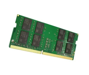
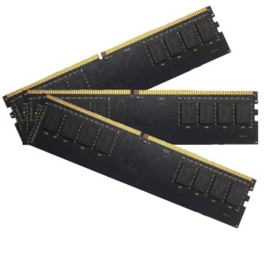
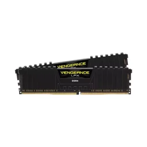
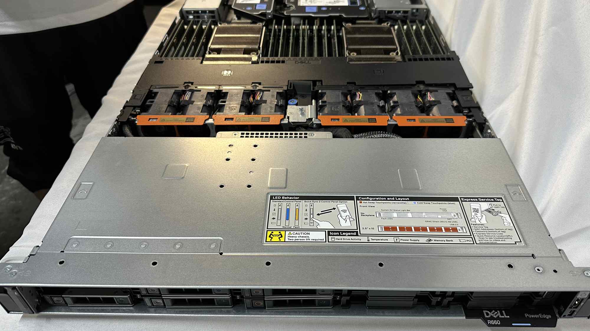
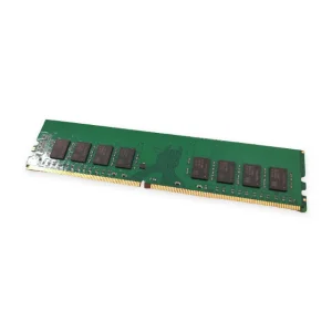
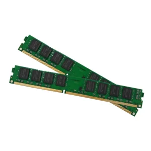
Modern memory modules like DDR5 (exemplified by our high-performance desktop memory series) and high-density computing systems demand stencils capable of printing for BGAs with pitches below 0.3mm. Our fine-grain steel stencils undergo automated electropolishing to reduce inner wall roughness, allowing consistent paste transfer for micro-BGA solder joints.
Industrial computing modules, system controllers, and automation boards often integrate fine-pitch logic devices beside heavy power components. This complex design requires stepped laser-cut stencils. Celtrix provides multi-level steps, combining variable thicknesses (e.g., 0.10mm, 0.12mm, and 0.15mm) on a single stencil panel with consistent step transitions.
How Celtrix implements rigorous verification matrices to conform to ISO and IPC standards.
Quality is the foundation of our engineering process. Celtrix maintains an ISO 9001:2015 Quality Management System managed by 56 dedicated quality control professionals. Our QA operations cover the entire production cycle, ensuring that every exported laser-cut stencil meets global electronics assembly standards.
Every batch of stainless steel sheeting undergoes hardness, tension, and chemical composition analysis to confirm compliance with ASTM and ISO benchmarks.
Our automated optical inspection systems check 100% of cut apertures against customer CAD data to identify variations in dimensions or edge quality.
All stencil designs are optimized around IPC-7525B stencil design guidelines, which establishes the baseline for modern global micro-component mounting.
Preparing the electronics manufacturing supply chain for upcoming shifts in PCB geometry.
As micro-LED displays, multi-chip packaging, and highly integrated power components reshape the layout of modern electronics, print design requirements are shifting. Celtrix is investing in several future technologies:
Addressing core SMT engineering questions regarding stencil performance, life span, and custom orders.
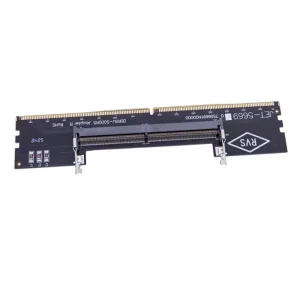
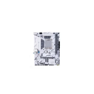
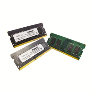
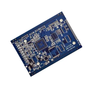
Browse our additional memory products, adapter cards, and advanced PCB assembly solutions.
 Celtrix Memory