Explore our key high-frequency multilayer PCBs, high-performance computing memory components, and industrial-grade modules.

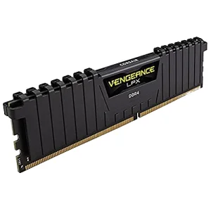
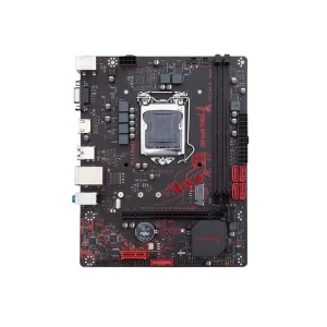
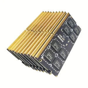
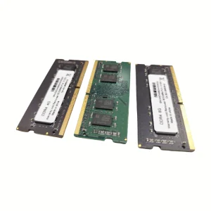
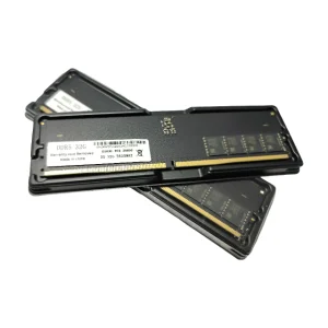
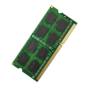
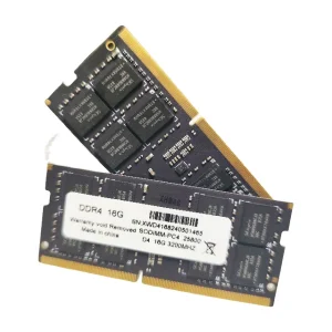
Analyzing industry shifts toward high-frequency substrates, miniaturization, and thermal efficiency.
Modern applications demand tighter routing. By utilizing blind vias, buried vias, and microvias, manufacturers increase component density, drastically shortening trace paths and reducing signal degradation in DDR5 and telecommunications hardware.
For high-speed designs operating at gigahertz speeds (like 6000MHz memory architectures), controlled differential impedance is vital. Advanced simulation tools configure copper weights and dielectric core parameters to curb crosstalk.
Multilayer structures use heavy copper layers, metal cores (such as aluminum backplanes), and thermal vias to pull heat away from active silicon, avoiding performance throttling in demanding server chips and high-power inverters.
As microprocessors push computational boundaries, Multi-layer Printed Circuit Boards have moved from passive carriers to active transmission lines. The integration of high-performance substrates like Rogers, Megtron 6, and high-Tg FR-4 represents the frontier of modern fabrication. Enterprises sourcing multi-layer PCBs must evaluate factories not merely on capacity, but on their ability to execute trace-width tolerancing within micro-level deviations, ensuring stable signal integrity across 12 to 32 layer stackups.
Global procurement teams must balance manufacturing cost with signal integrity, substrate reliability, and supply-chain transparency. Our manufacturing framework covers these critical considerations:
By coordinating component sourcing, raw base laminates, and final testing under one production canopy, we minimize logistics friction and secure faster turnaround for critical industrial components.
Our structural guidelines and execution protocols comply with international metrics for high-reliability electronics:
| Parametric Attribute | Standard Capability | Advanced Tolerances |
|---|---|---|
| Max Layer Count | 2-16 Layers | 18-32 Layers |
| Trace Width / Spacing | 3.5 mil / 3.5 mil | 3 mil / 3 mil (HDI) |
| Aspect Ratio | 8:1 | 12:1 |
| Impedance Control | ±10% | ±5% |
| Quality Classification | IPC Class 2 | IPC Class 3 (Medical/Aero) |
Combining production automation with vertical integration to mitigate market volatility and logistical bottlenecks.
Unlike single-focus PCB shops, our facility integrates high-precision board manufacturing, component SMT (Surface Mount Technology), and system-level test services. We control the process from raw base copper clad laminates to functional testing of complex systems like DDR5 high-speed memory arrays and server motherboards.
We deploy smart warehouse software integrated with automated SMT placement machines. Crucial components are tracked dynamically, minimizing inventory errors and ensuring tracking accountability throughout the manufacturing cycle.
Advanced optical (AOI), 3D X-ray (AXI), and in-circuit tests (ICT) dynamically report layout performance anomalies. This data is fed back to placement machines to constantly adjust configurations and prevent manufacturing variations.
By integrating memory chip mounting, multi-layer high-frequency PCB board fabrication, and complex controller assembly under one roof, we significantly shorten international supply chains. This setup reduces logistics transit steps, avoids split-responsibility disputes, and delivers a unified warranty from a single partner.
From high-capacity server infrastructure to industrial power inverter controls.
Industrial data centers rely on low-loss material, high-layer-count backplanes. Our multilayer PCBs support critical layouts for DDR5 and DDR4 memory modules, handling signals from 3200MHz to 6000MHz with low impedance and minimal signal loss.
For systems handling high voltages and currents, like power bank arrays and welding machine inverters, heavy copper layers are essential. These designs prevent localized heating, ensuring safe, continuous industrial operation.
Smart IoT devices and power banks pack complex Wi-Fi controllers, charging logic, and status displays onto tiny, multi-layered circuit boards. Compact stackups and microvias allow these dense boards to fit into small consumer enclosures.
A trusted manufacturer specializing in high-performance DRAM solutions, motherboards, and integrated multi-layer PCB assemblies.
Established in 2017, Celtrix Memory Technologies Co., Ltd. specializes in engineering and exporting high-performance memory modules, motherboards, and complex PCB assemblies. We support client requirements across industrial, server, consumer, and embedded hardware fields.
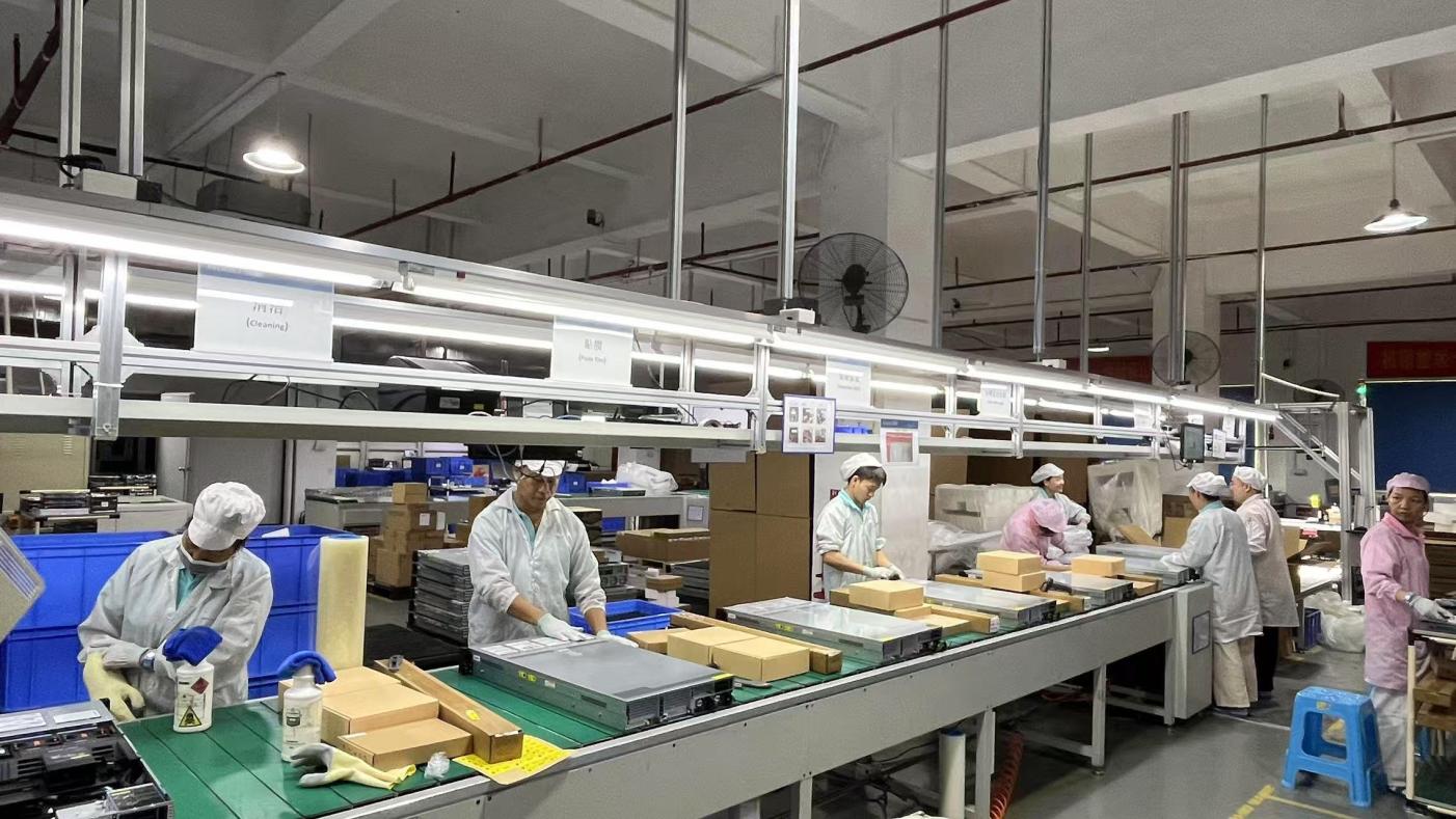
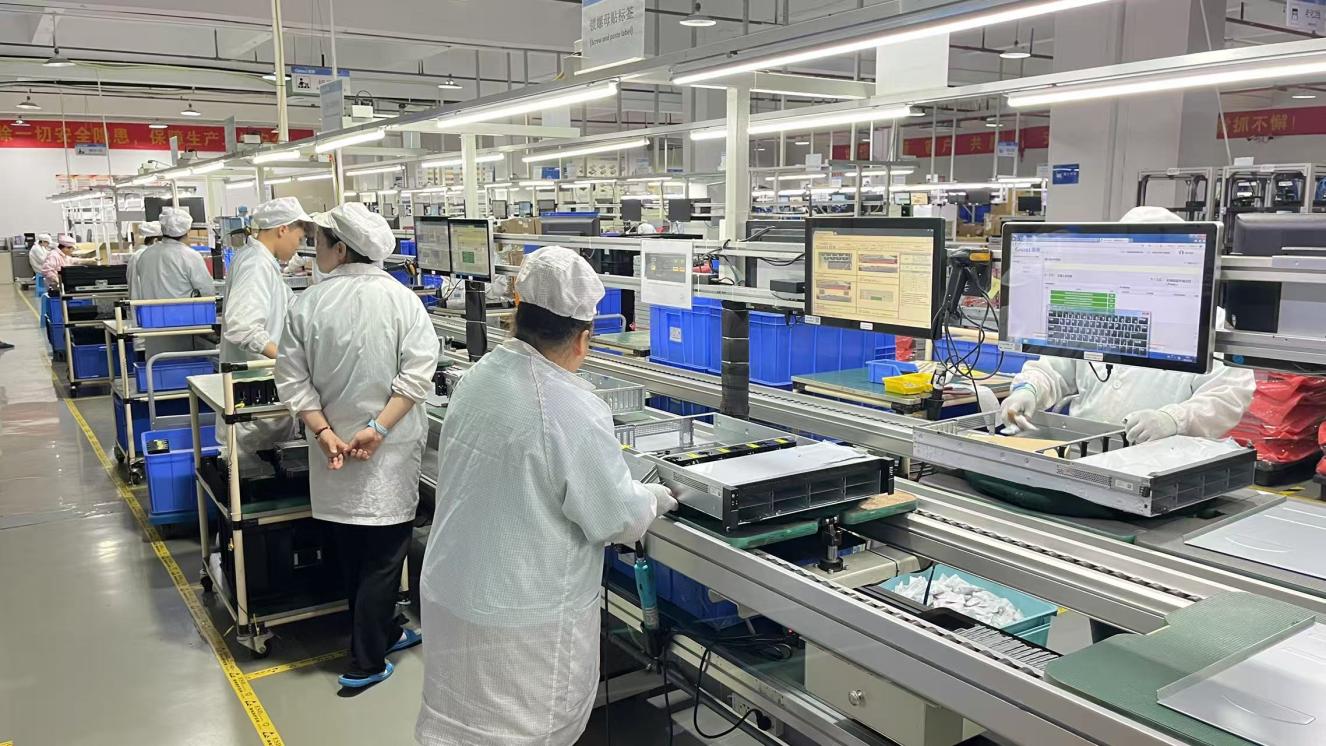
Our modern 28,600 m² factory houses automated SMT lines, advanced reflow ovens, and precise optical testing. These capabilities allow us to manage every step from board fabrication to component assembly, ensuring consistent quality and reliable performance.
Drawing on 9 years of industry experience and 7 years of exporting to over 50 countries, we generate more than USD 23 million in annual export revenue. This stable operation is supported by robust logistics, technical support, and comprehensive OEM/ODM services.
Our quality control processes ensure that all PCB arrays and memory assemblies perform reliably under demanding conditions.
Incoming inspection verifies substrate thickness, copper foil quality, and passive components. X-ray fluorescence checking validates surface finishes.
Automated Optical Inspection scans printed layouts before and after surface-mount reflow to flag solder voids, bridge defects, and component alignment issues.
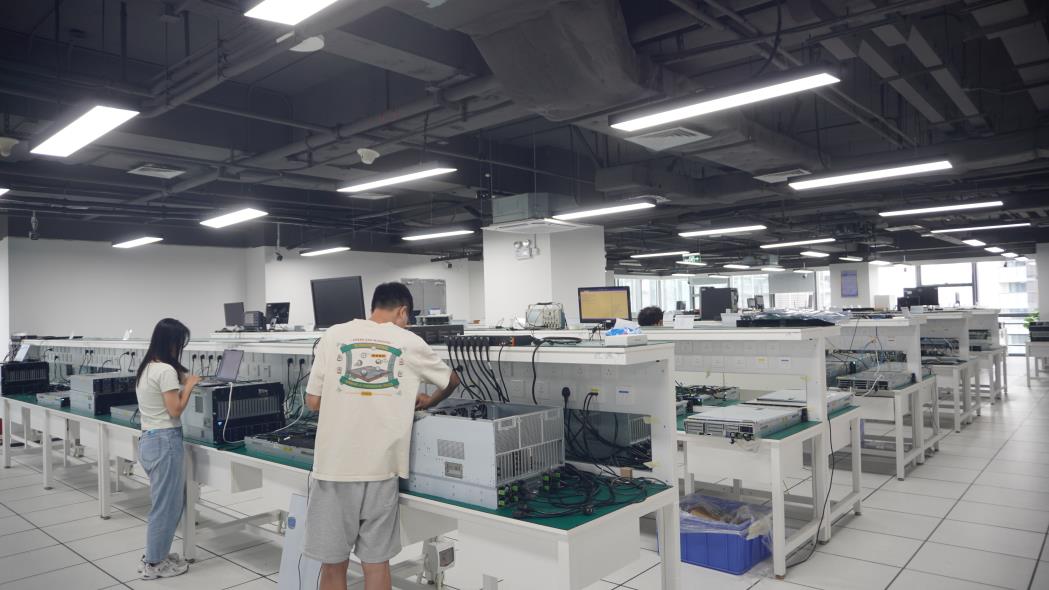
Assembled boards undergo functional testing. Server modules and components are subjected to thermal stress testing to identify and eliminate early-life failures.
Final Quality Control checks physical dimensions, verifies compliance with customer specifications, and confirms vacuum packaging is sealed to prevent oxidation.
Get answers to common technical and logistical questions about sourcing multi-layer PCBs and hardware assemblies.
High-Tg materials (Tg ≥ 170°C) maintain their structural stability, mechanical strength, and electrical properties under elevated temperatures. This makes them ideal for multi-layer PCBs subjected to lead-free soldering profiles and high-temperature environments, preventing delamination and traces separating from the board.
We use modern impedance simulation software to calculate exact trace dimensions based on the dielectric constant (Dk) of the prepreg and core material. During manufacturing, we use flying-probe test fixtures to verify and maintain impedance tolerances within ±5% or ±10%, according to customer specifications.
IPC Class 2 is the standard for general industrial and consumer electronics where continuous performance is expected but not critical. IPC Class 3 requires stricter tolerances, thicker plating in vias, and cleaner manufacturing. It is used for medical equipment, aerospace hardware, and key infrastructure where downtime is not acceptable.
Yes. Our SMT production lines are equipped to mount fine-pitch BGAs, PMIC chips, and high-frequency memory components required for DDR5 modules. This process is monitored by 3D optical and X-ray inspection to ensure reliable solder connections.
ENIG (Electroless Nickel Immersion Gold) is recommended for flat surfaces, fine-pitch components, and long shelf life. HASL Lead-Free is a cost-effective option for less complex designs, while OSP (Organic Solderability Preservatives) is commonly chosen for simple, high-volume production.
We provide comprehensive customization, including tailored PCB layout adjustments, multi-layer stackup design, custom heatspreaders, SPD programming, custom packaging, and private label services to meet specific brand requirements.
Complete your hardware solutions with our high-speed DDR4, DDR5 memory components, and compatible system boards.
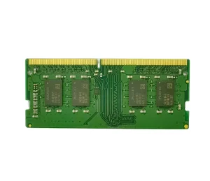
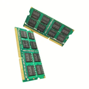
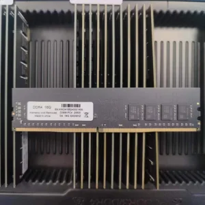
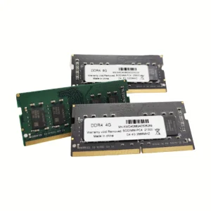
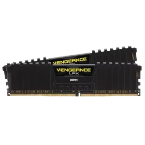
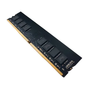
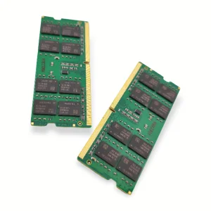
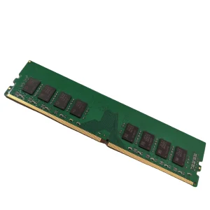
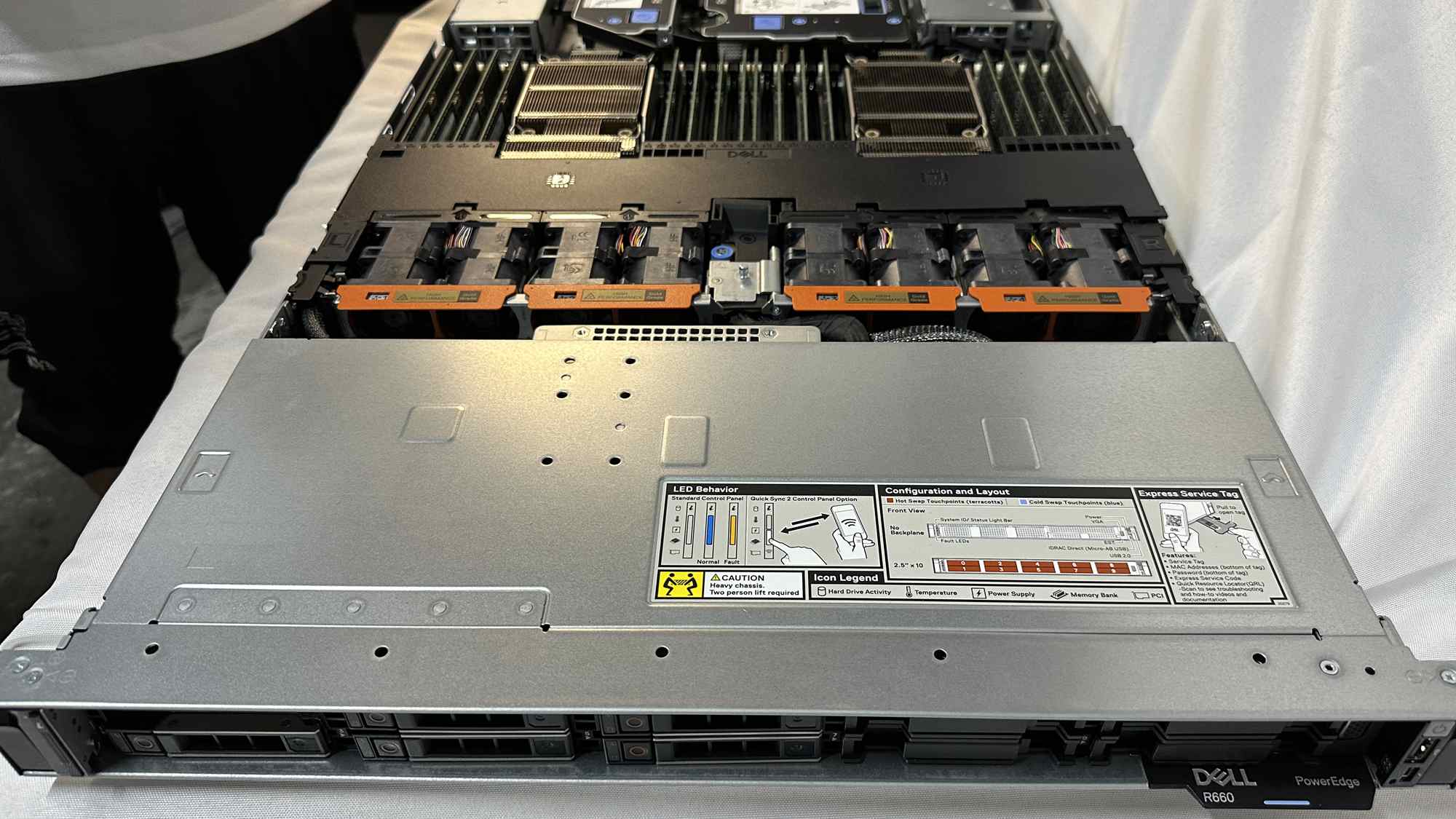
Step inside our manufacturing areas, showing where raw substrates are transformed into tested multi-layer hardware.

 Celtrix Memory