Explore our high-performance printed circuit boards, custom assembly solutions, and industrial-grade modules engineered to meet strict international standards.
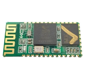
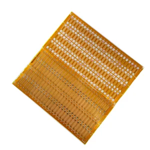
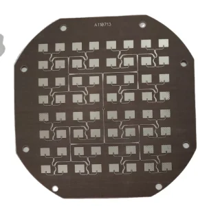


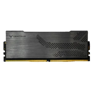
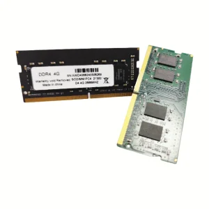
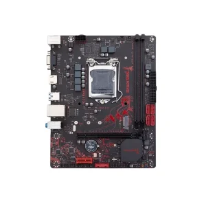
In modern electronic design, selecting the optimal substrate configuration is critical to system efficiency, signal integrity, and cost-effectiveness. As premier PCB Double/Single Sided PCBs Manufacturers & Exporters, Celtrix Memory Technologies Co., Ltd. supplies high-precision substrates engineered for demanding applications. While multi-layer boards dominate high-density processor boards, single and double-sided PCBs remain the bedrock of the global electronics industry, balancing manufacturing simplicity with outstanding electromagnetic performance.
Composed of a single conductive copper layer laminated onto a rigid non-conductive dielectric substrate (often FR-4, CEM-1, or metal core aluminum). Ideal for cost-sensitive, low-frequency applications like power adapters, sensor systems, and basic consumer electronics.
Features conductive traces etched onto both top and bottom layers of the dielectric substrate. Interconnection between trace paths is achieved through Plated Through-Holes (PTH) or microvias. Essential for higher component density, shielding tracks, and moderate-frequency applications.
Utilizes high-TG FR-4, Taconic high-frequency laminates, and advanced surface finishes such as Electroless Nickel Immersion Gold (ENIG), Hot Air Solder Leveling (HASL), and Organic Solderability Preservatives (OSP) for superior solder joint integrity.
Design engineers must evaluate multiple physical properties when choosing materials for single or double-sided PCBs:
As global supply chains demand shorter lead times and higher precision, partnering with an established manufacturer in China provides structural competitive advantages. The dense concentration of material suppliers, raw chemical fabricators, and advanced component markets yields unmatched speed and capability.
China's PCB manufacturing cluster coordinates raw substrate production (FR-4, CEM-3, Polyimide, Copper Clad Laminates) alongside advanced tooling, chemical suppliers, and automated assembly operations. This spatial concentration eliminates logistics bottlenecks, enables rapid-turn prototyping within 24 to 48 hours, and supports transition to high-volume manufacturing without multi-continental shipping delays.
Modern Chinese facilities utilize state-of-the-art Direct Imaging (LDI) technology, Automated Optical Inspections (AOI), and precise high-speed CNC drilling. By automating critical lamination and trace etching steps, production centers achieve micro-precision tolerances down to 3 mil (75 microns) trace width and spacing. This guarantees consistent electrical properties across large export shipments.
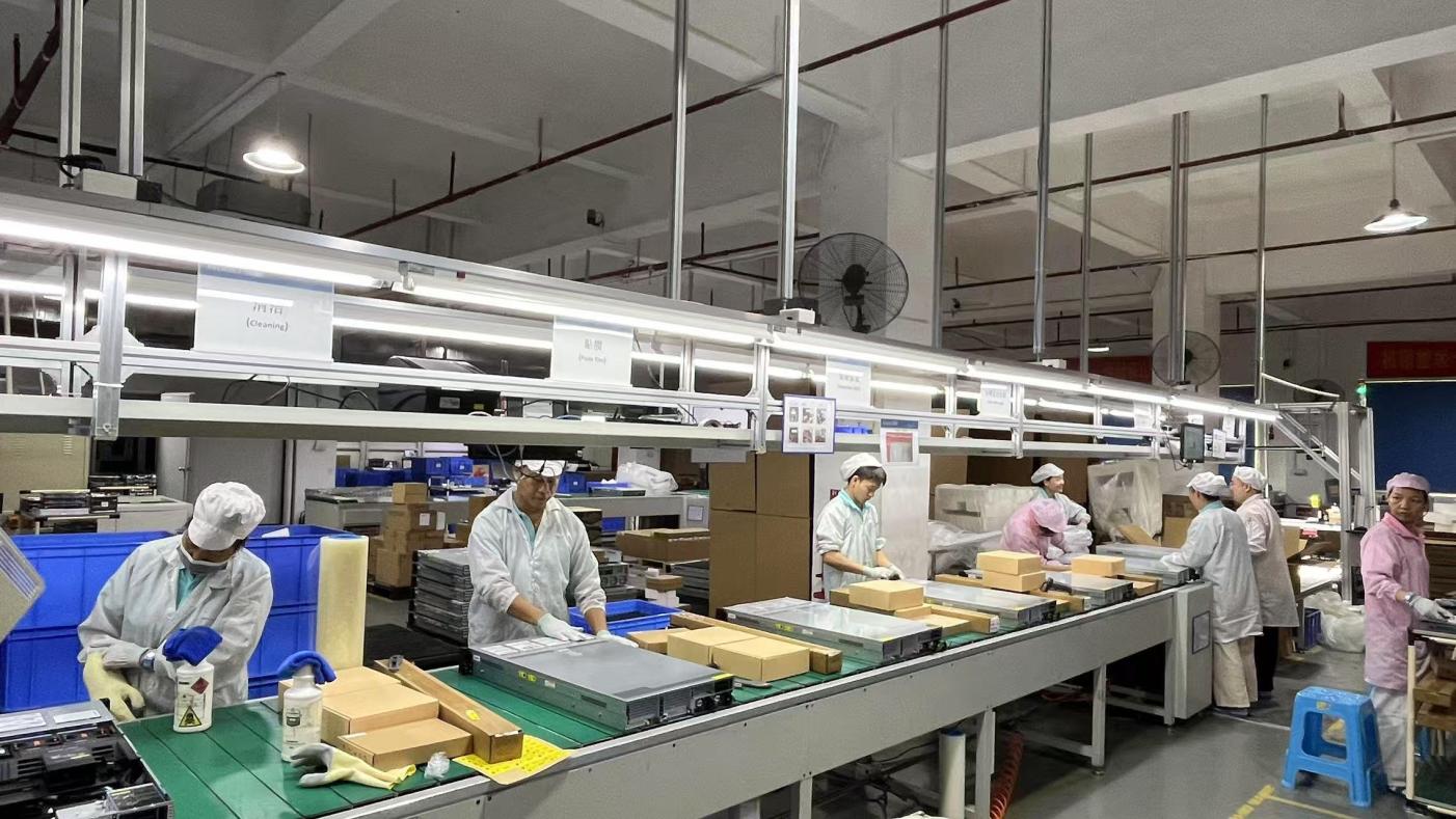
Additionally, the geographic alignment of PCB fabrication with world-class surface mount technology (SMT) packaging facilities—like Celtrix’s modern industrial facilities—ensures that bare boards are transferred to assembly lines without environmental contamination, preserving pad solderability and preventing oxidation.
Celtrix Memory Technologies Co., Ltd. is a professional DDR5 memory and high-performance electronics manufacturer dedicated to delivering high-reliability solutions for global customers. Since its establishment in 2017, the company has integrated advanced printed circuit board designs, SMT operations, and final packaging processes.
Operating within strict compliance to the ISO 9001 Quality Management System, Celtrix employs 56 certified quality control professionals. Every double-sided and single-sided PCB design or assembled module undergoes rigorous testing, including Incoming Material Inspection (IQC), In-Process Quality Control (IPQC), Automated Optical Inspection (AOI), Functional Testing, Burn-in Test, Aging Test, and Final Quality Control (FQC).
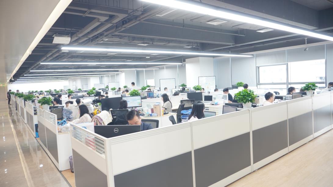
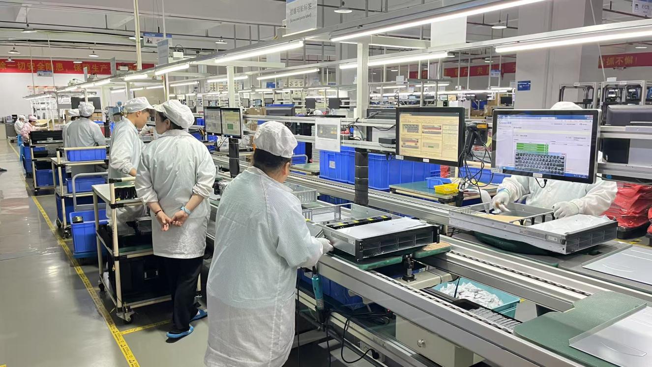
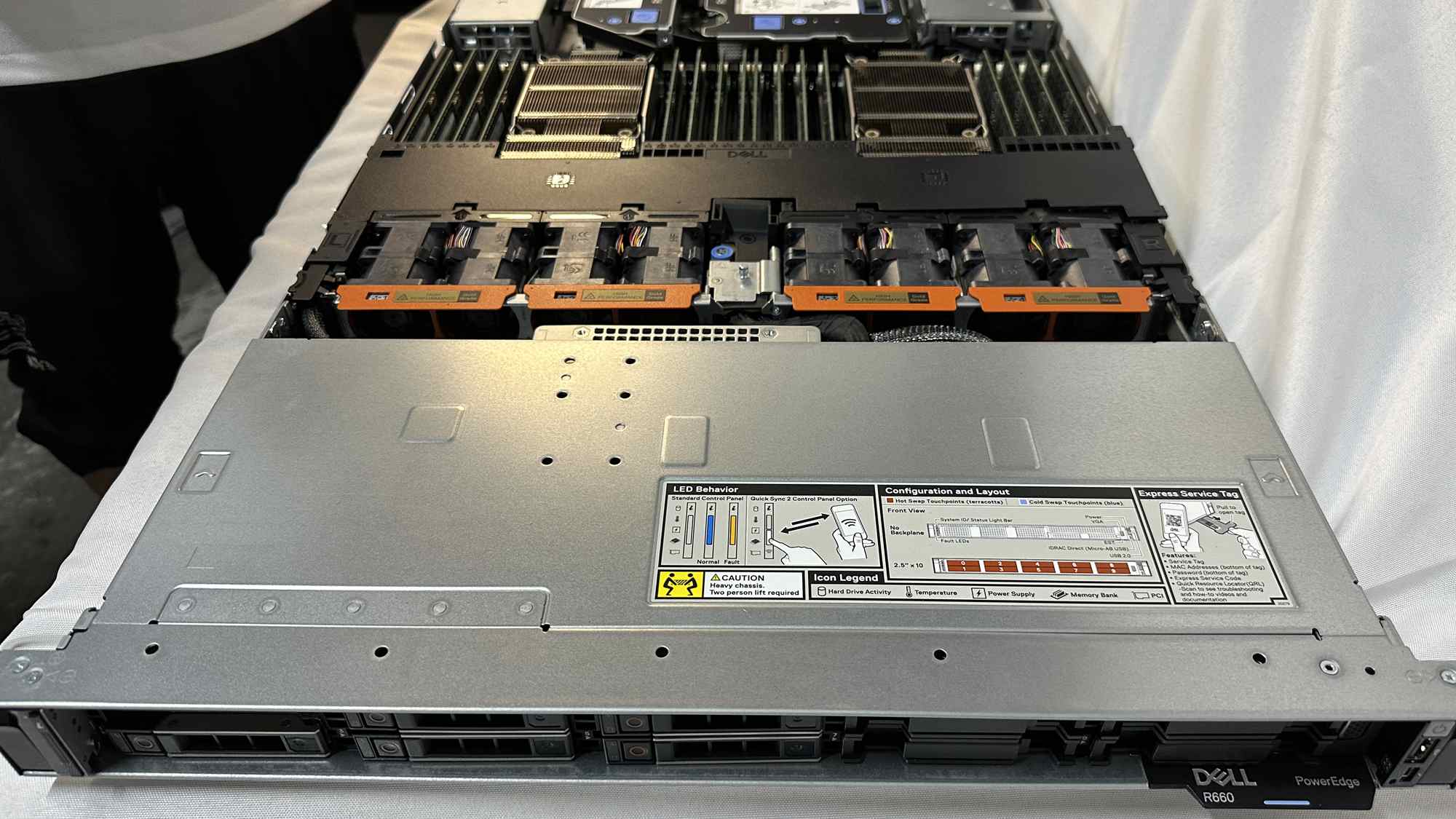
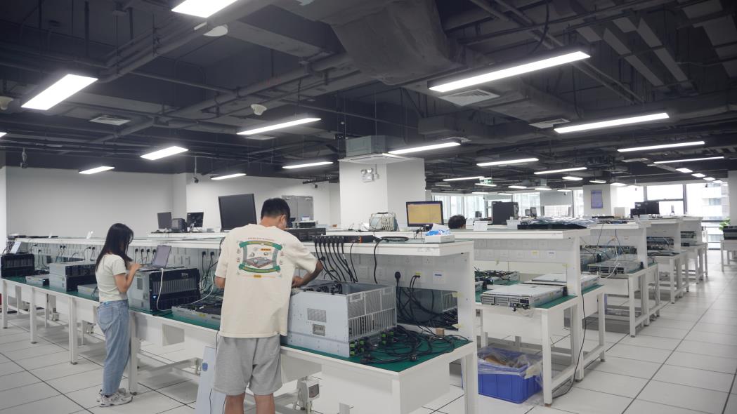
PCB technology is not one-size-fits-all. Different industries require customized trace structures, substrate metals, and component layouts to withstand environmental stressors and electrical requirements.
Industrial environments present extreme mechanical vibrations and electromagnetic interference (EMI). High-sensitivity assemblies, such as those used in metal detection systems, require double-sided designs with dedicated ground planes to shield sensitive analog circuitry from signal distortion.
For aerospace, satellite receivers, and wireless infrastructure, dielectric loss must be minimized. Incorporating high-frequency Taconic substrates (such as Taconic TLY-5) provides a low dissipation factor and stable dielectric constant across temperature ranges, optimizing high-speed transmission lines.
Thermal dissipation is key in power converters, automotive drive systems, and high-power LED installations. Metal core PCBs (MCPCBs) using aluminum substrates effectively conduct heat away from surface components, extending system lifespan and preventing failure from thermal runaway.
Enterprise-level purchasers look beyond unit costs; they prioritize supplier reliability, supply chain resilience, compliance, and custom design capabilities.
Modern global brands require engineering support that can transition from double-sided prototype breadboards to high-speed automated production. By providing comprehensive ODM/OEM capabilities, Celtrix supports rapid transition periods through precise Gerber file reviews (DFM check), ensuring that design errors are mitigated before layout etching occurs.
From logo printing, custom copper weight specifications (from 0.5 oz to 4 oz), solder mask color choices (green, blue, black, white), to custom SPD programming for memory-integrated board structures, having a customizable electronics supplier simplifies integration, allowing system builders to market branded, market-ready solutions.
Exporting to highly regulated markets like Europe and North America demands adherence to environment and safety standards. High-tier manufacturers guarantee compliance with the RoHS and REACH directives (ensuring lead-free materials) and hold UL certifications for safety performance.
The printed circuit board industry is undergoing a significant transformation driven by high-speed data transmission, industrial IoT, and the electrification of vehicles.
As consumer devices shrink, the need for High-Density Interconnect (HDI) structures grows. Manufacturers are deploying thinner core materials, microvias, and fine-line routing to maximize surface space on double-sided boards, allowing complex circuitry to fit within small envelopes.
Embedding resistors and capacitors directly inside the internal layers of double-sided boards helps reduce surface clutter, frees up board space for active silicon components, improves signal integrity, and minimizes parasitic inductance at high operating frequencies.
Global demand is driving the industry toward eco-friendly fabrication processes. This includes adopting halogen-free laminates, recycling chemical solutions, reducing water consumption during etching, and implementing lead-free hot-air solder leveling options.
Find expert answers to common queries regarding single-sided and double-sided PCB layout design, substrate materials, and procurement procedures.
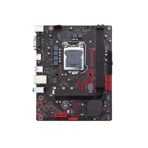
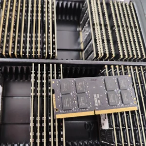
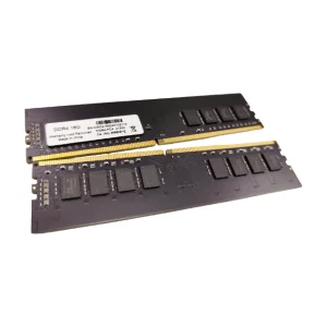
Discover our high-capacity RAM memory modules, multi-layer motherboard solutions, and specialized industrial PCBA designs.
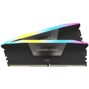
 Celtrix Memory