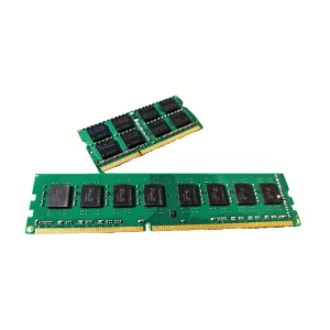
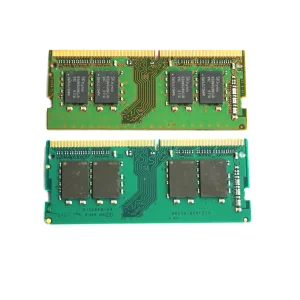
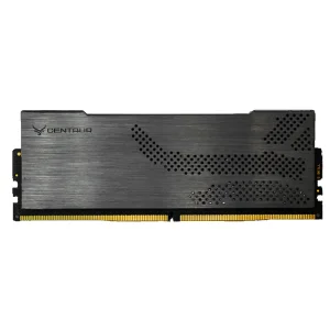
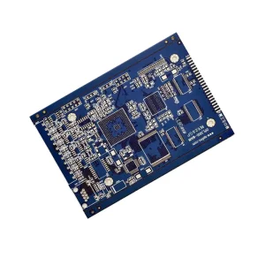
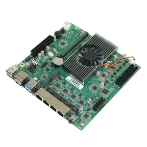
Explore our core manufacturing array, spanning high-conductivity printed circuit boards, high-speed DRAM modules, and server-grade compute units.
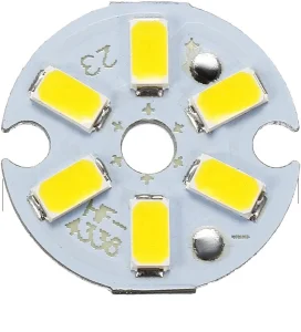
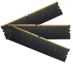
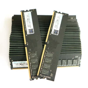
In high-power illumination, horticultural lighting, automotive displays, and advanced optical communication, the printed circuit board (PCB) is far more than a simple structural mount. It serves as the primary thermal dissipation path. High-power LEDs generate significant localized thermal loads; without an engineered dissipation mechanism, junction temperatures rise rapidly, causing luminance degradation, wavelength shifting, and premature chip failure.
Modern LED PCB factories utilize Metal Core PCBs (MCPCBs), particularly aluminum and copper clads, alongside high-performance FR4 designs featuring thermal via arrays. By embedding a dielectric polymer layer with high thermal conductivity between the circuit copper and the metal base plate, modern manufacturing processes achieve thermal conductivity ranges from 1.0 W/m-K up to 8.0 W/m-K. This design provides structural support while keeping the LED junction temperatures well within safe operating limits.
Celtrix Memory Technologies Co., Ltd. – Leading EMS Solutions and Semiconductor Integration
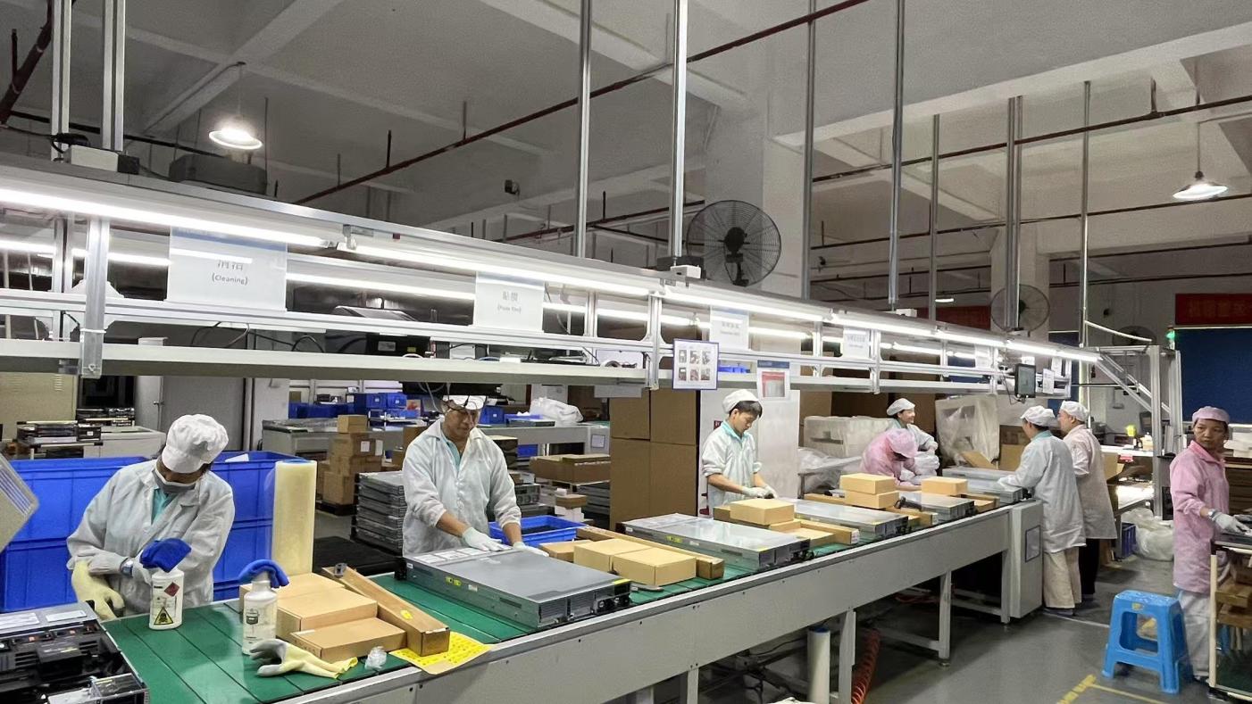
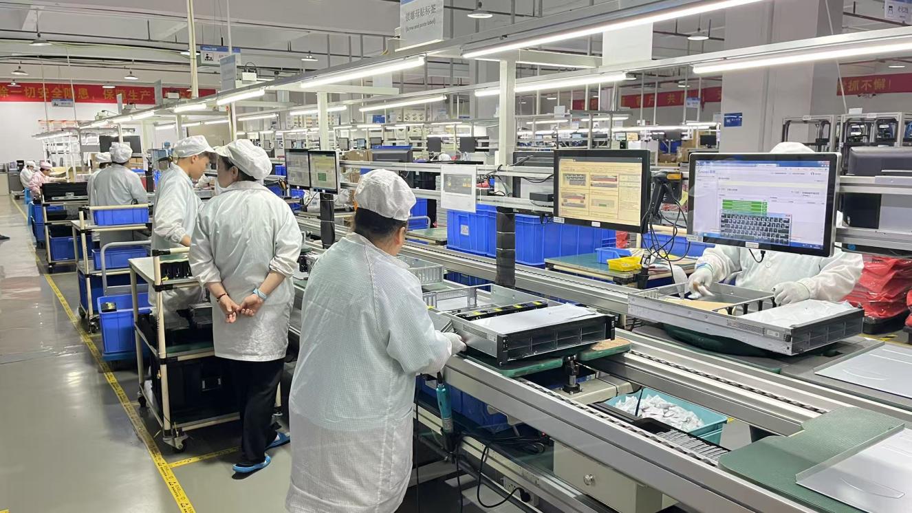
Established in 2017, Celtrix Memory Technologies Co., Ltd. has developed into a high-capacity OEM/ODM partner for global high-technology enterprises. Operating a state-of-the-art 28,600 m² manufacturing facility, Celtrix leverages advanced SMT assembly lines, automated optical inspection (AOI) suites, and cleanroom production enclosures to fabricate complex multi-layer PCBs, advanced memory modules, and custom PCBA systems.
With over 9 years of industry experience and 7 years of direct export experience spanning more than 50 countries, we understand the technical and regulatory requirements of the North American, European, and Asian markets. Supported by 142 dedicated R&D engineers, Celtrix ensures every production run—from quick-turn prototypes to high-volume multi-layer structures—meets strict quality control standards.
Our quality management workflow operates under ISO 9001 certification. Every production batch undergoes a series of inspections including Incoming Material Inspection (IQC), In-Process Quality Control (IPQC), Automated Optical Inspection (AOI), functional diagnostics, thermal burn-in, aging analysis, and Final Quality Control (FQC) managed by 56 dedicated QA professionals.
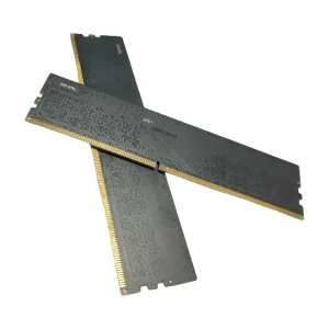
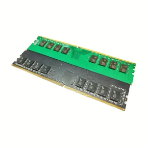
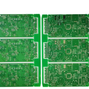
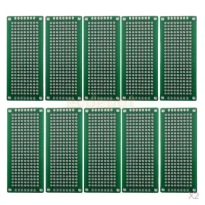
Whether you require multi-layer FR4 boards for IoT controllers, high-conductivity metal core substrates for industrial LED arrays, or high-performance DDR4/DDR5 memory modules, Celtrix delivers industrial-grade components designed to perform reliably under demanding conditions.
Key insights into technological shifts, material specifications, and global sourcing strategies.
The industry is transitioning toward high-density MiniLED and MicroLED arrays. These require precise sub-100µm space/trace routing, advanced solder mask alignment, and stable substrate flatness to allow high-yield SMT component placement.
Demanding industrial applications now utilize ceramic-filled polymer dielectric layers, allowing MCPCBs to operate continuously at high temperatures without delamination or dielectric breakdown.
Automotive headlamps and daylight running lights require compliance with strict standards. Factories must adhere to IPC-A-610 Class 3 workmanship criteria and pass rigorous thermal cycling tests.
| Substrate Material Class | Thermal Conductivity (W/m-K) | Dielectric Breakdown Voltage | CTE (ppm/°C) (X/Y axis) | Primary Industrial Applications |
|---|---|---|---|---|
| Standard FR-4 (with thermal vias) | 0.3 – 0.5 (Via dependent) | > 40 kV/mm | 14 – 17 | Low-power consumer indicators, IoT displays, control panels. |
| Aluminum Metal Core (MCPCB) | 1.0 – 3.0 | 2.0 – 6.0 kV AC | 22 | Commercial streetlights, stadium floods, architectural washes. |
| Copper Base MCPCB (Direct Thermal Path) | 4.0 – 8.0+ | Not applicable (Direct bonding) | 17 | High-power automotive headlights, projection systems, stage spots. |
| Ceramic Base (Al2O3 / AlN) | 24 – 180 | > 15 kV/mm | 5 – 7 | High-power UV-C purification arrays, laser diodes, aerospace. |
The global electronics sector relies on advanced manufacturing ecosystems. Chinese LED PCB factories have evolved beyond labor-intensive assembly, transitioning to digital smart manufacturing (Factory 4.0). Integrated manufacturing executions systems (MES) coordinate with ERP pipelines to track every component, from raw metal sheets to the finished, tested board assembly.
This ecosystem offers distinct advantages for global procurement teams:
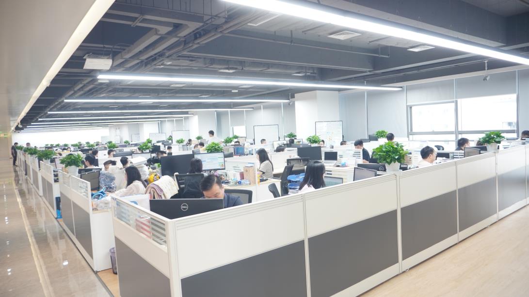
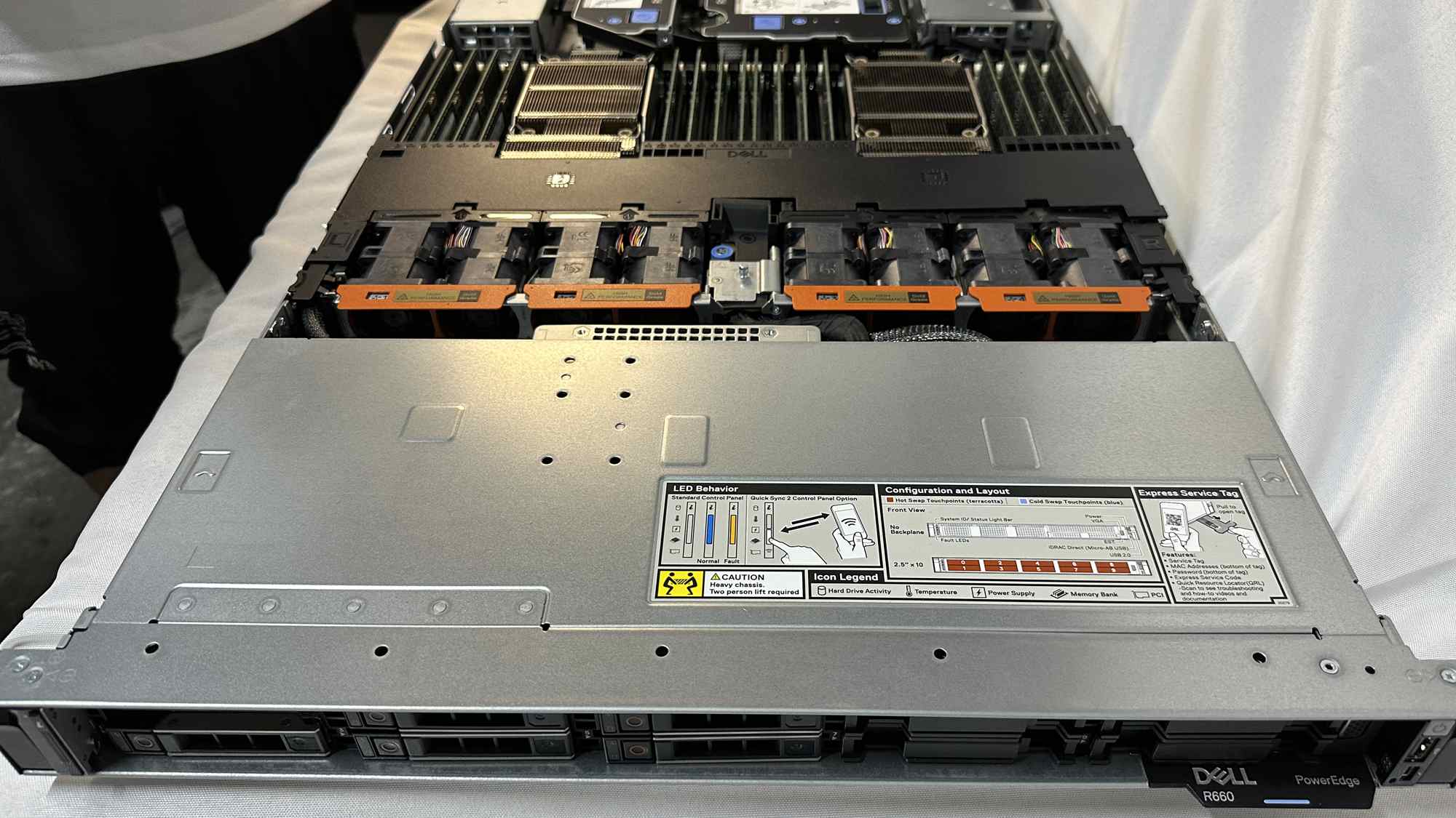
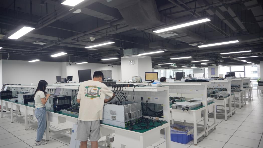
Our integrated manufacturing facilities are organized to maintain quality and reliability at scale. The factory floor photos below show our SMT lines, precision testing areas, and warehousing systems.
Adapting LED PCB technology to regional regulations, environmental challenges, and industry demands.
Primary Focus: High-performance architectural lighting, horticultural grow arrays, and automotive assemblies.
Compliance Requirements: UL 796, UL 94V-0 flammability certification, FCC Part 15 class B compatibility, and DLC (DesignLights Consortium) standards for commercial lighting efficiency.
Primary Focus: Low-carbon streetlighting, municipal transit indicators, and industrial automation control displays.
Compliance Requirements: Strict RoHS and REACH declarations, CE directives, EN 62031 photobiological safety standards, and WEEE waste diversion guidelines.
Primary Focus: High-volume consumer electronics, smart home appliances, and display backlights.
Compliance Requirements: CCC (China), PSE (Japan), KC (Korea), and custom safety marks focused on durability under humid environments.
Technical answers to key PCB and LED PCB manufacturing questions.
Review our complete range of certified hardware, memory solutions, and processing boards.
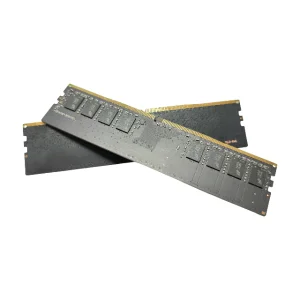
 Celtrix Memory