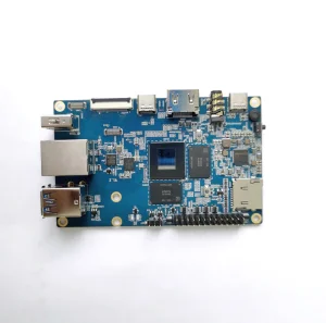
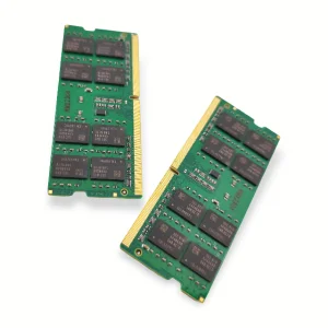
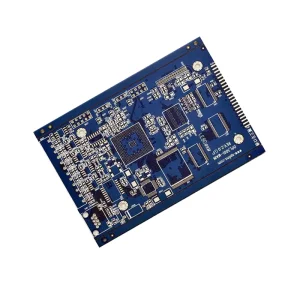
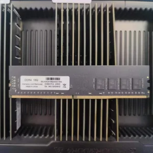
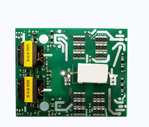
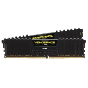
Explore our foundational range of hardware configurations, built using premium high-frequency layouts and robust sub-assemblies.
An in-depth review of industrial applications, thermal thermodynamics, stack-up optimization, and fabrication methodologies.
The global push for electrification, clean energy storage, high-power industrial equipment, and electric vehicles (EVs) has dramatically increased the demand for Heavy Copper PCBs (defined as boards with ≥3 oz/ft² of copper). Standard consumer electronics typically rely on 1 oz copper weights, which are incapable of handling high current loads and extreme thermal cycles. In contrast, thick copper PCBs provide the physical infrastructure necessary to withstand massive energy surges without risking delamination, open-circuits, or thermal degradation.
Modern power distribution systems generate intense localized heat. By upgrading to thick copper, engineers gain access to a larger cross-sectional area, which significantly lowers the electrical DC resistance ($R = \rho L / A$) and minimizes internal heat losses ($P = I^2 R$). This transition reduces the operating temperature of critical power converters, industrial drives, and traction control modules, directly enhancing overall system durability and system efficiency.
Heavy copper allows manufacturers to combine high-power circuits with control circuitry on a single, consolidated substrate. This eliminates complex hand-wired connectors, reduces the overall physical volume of the final housing, and improves signal integrity. Combining thick copper with automated Surface Mount Technology (SMT) enables the dense population of high-performance components (like MOSFETs and IGBTs) on a unified thermal base.
Designing heavy copper circuits requires strict adherence to physical limitations. As copper thickness increases, chemical etching leaves a characteristic trapezoidal slope on trace walls, meaning the trace width must be dynamically adjusted during layout. According to IPC-2152 standards, selecting the correct trace width is critical to keep the temperature rise ($\Delta T$) within acceptable margins.
| Copper Weight (oz/ft²) | Nominal Thickness (µm / mil) | Min. Trace Width (mil) | Min. Air Gap (mil) | Typical Application |
|---|---|---|---|---|
| 3 oz | 105 µm / 4.2 mil | 10 mil | 12 mil | High-output SMT Converters, Servers |
| 4 oz | 140 µm / 5.5 mil | 12 mil | 14 mil | Industrial Drives, EV Chargers |
| 6 oz | 210 µm / 8.3 mil | 15 mil | 18 mil | Power Distribution Blocks, Wind Turbines |
| 10+ oz | 350+ µm / 13.8+ mil | 25 mil | 30 mil | Extreme Military Systems, Arc Welders |
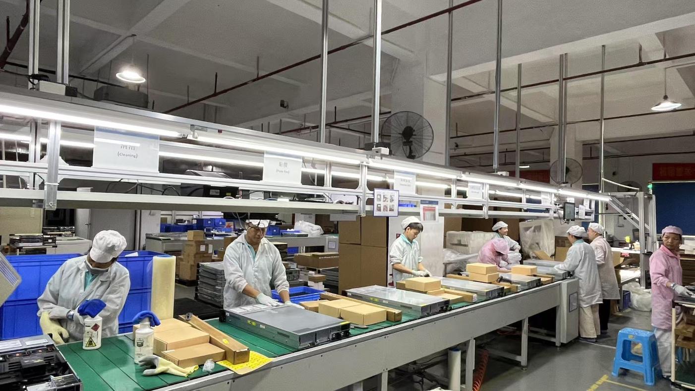
Celtrix Memory Technologies integrates precision PCB processing and high-speed SMT assembly within a certified, modern industrial facility.
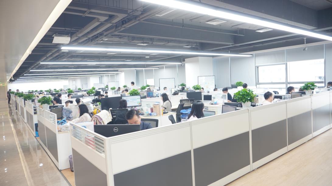
Founded in 2017, Celtrix Memory Technologies Co., Ltd. has developed from a dedicated high-performance DRAM manufacturer into a comprehensive electronics manufacturing group. We combine precision SMT automation with advanced multi-layer and heavy copper PCB processing to serve clients in more than 50 countries.
Operating a state-of-the-art 28,600 m² facility, we support the entire production cycle, from initial CAD layout review and thermal simulation to raw substrate processing, SMT, wave soldering, and final burn-in testing. This integrated workflow guarantees that your heavy copper substrates are fully compatible with your electronic assemblies.
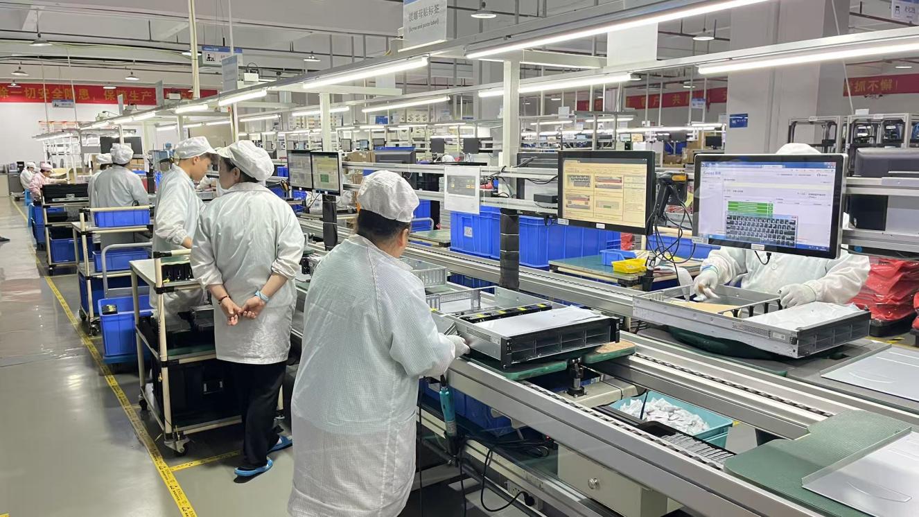
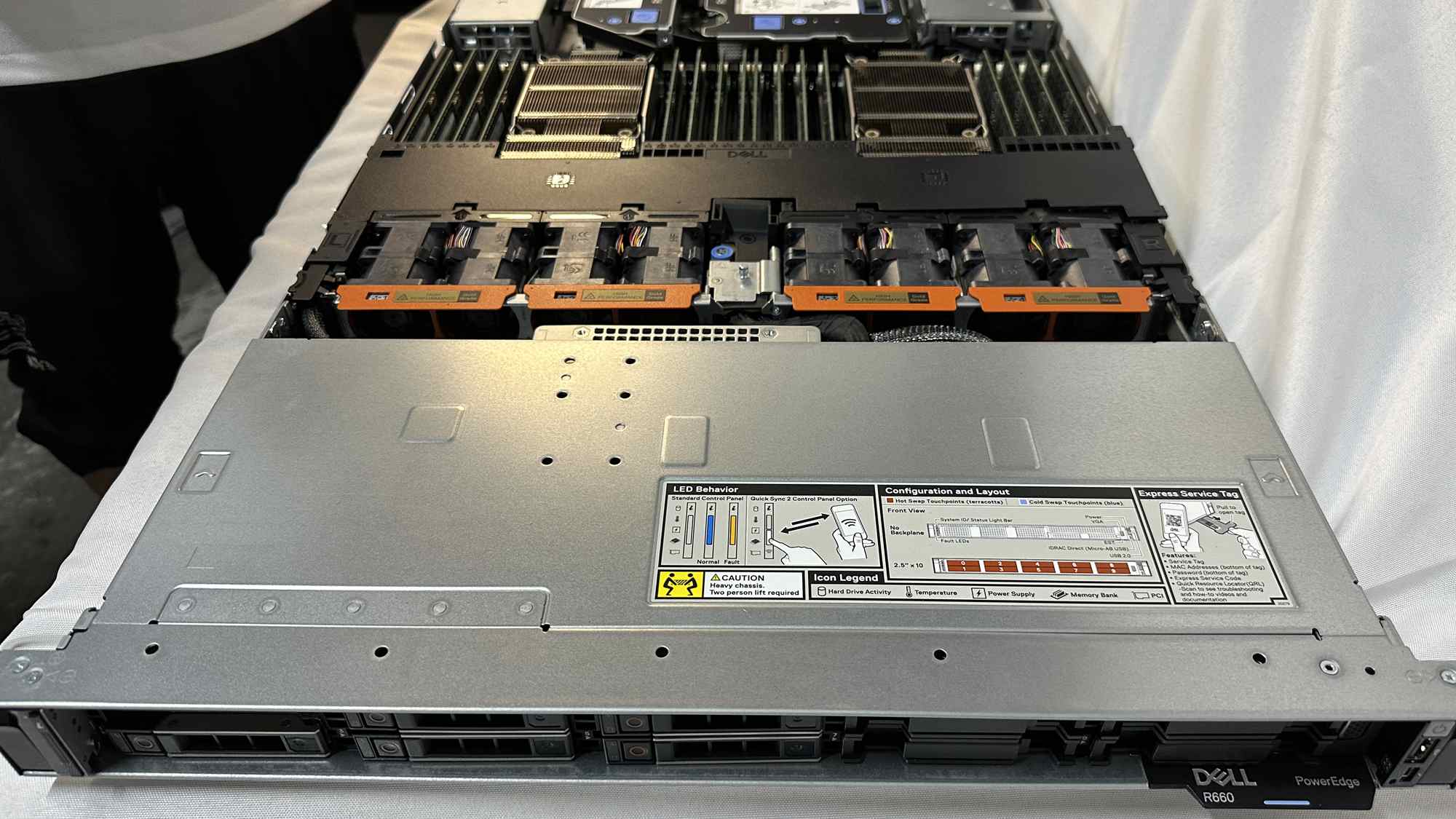
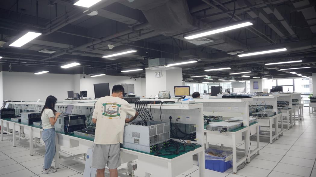
Thick copper printed circuit boards are essential components in demanding industrial and automotive applications. Our assemblies are manufactured to meet international standards, ensuring reliability in high-stress operational environments.
EV & Hybrid Powertrains: Main drive traction inverters, onboard battery chargers, and high-voltage DC-DC converters require heavy copper layers (often 4 oz or greater) to handle hundreds of amperes while maintaining low internal thermal rise.
Renewable Energy Systems: Solar micro-inverters, wind turbine power modules, and grid-scale energy storage systems rely on thick copper boards to manage continuous high currents and resist environmental temperature shifts.
Industrial Power Supplies & Welder Systems: High-frequency welding machinery, heavy-duty motor controllers, and uninterruptible power supplies (UPS) use heavy copper traces to prevent track burnout and structural failure under load.
Our heavy copper boards and integrated assemblies undergo rigorous qualification testing to satisfy international specifications:
Innovation continues to drive the electronics industry. Here is how heavy copper technology is evolving to meet tomorrow's power demands.
AI accelerators and high-power compute clusters require power distribution networks (PDN) capable of handling transient currents over 1000A. We are developing hybrid thick copper stackups that place thick, high-current copper layers alongside fine-pitch signal layers, supporting both power delivery and high-speed data on the same board.
Embedding active and passive components within the inner layers of the PCB helps minimize path inductance and overall footprint. We are researching methods to embed heavy copper bus bars directly into multi-layer substrates, improving thermal performance for automotive and industrial modules.
Chemical waste management is a key focus in thick copper production. We are updating our manufacturing facilities with closed-loop copper reclamation systems. These systems recycle acidic etchant solutions and reclaim dissolved copper, reducing the environmental footprint of our PCB manufacturing processes.
Review engineering guidelines, design rules, and manufacturing constraints for high-power electronics projects.
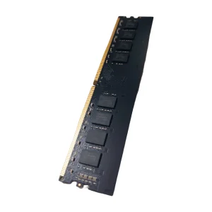
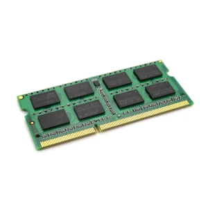
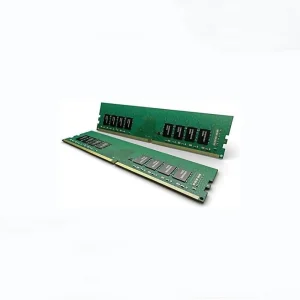
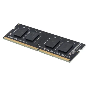
Explore our additional component configurations, including advanced memory kits and industrial inverter boards designed for high reliability.
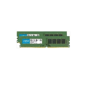
 Celtrix Memory