Premium OEM assemblies customized for high-reliability consumer electronics, edge computing node installations, and heavy-duty industrial systems in Incheon and Seoul.
Analyzing the strategic intersection of memory integration, automotive-grade standards, and high-frequency PCBs within the Gyeonggi-do and Pangyo Techno Valleys.
South Korea stands as an undisputed global titan in high-end semiconductor fabrication and display technologies. Driven by industrial giants such as Samsung Electronics, SK Hynix, and Hyundai Motors, the local electronics hardware infrastructure requires highly specialized, Tier-1 Printed Circuit Board Assemblies (PCBAs). The localized electronic ecosystem is heavily clustered around areas like Pangyo Techno Valley (Korea's Silicon Valley), Gumi Industrial Complex, and the Incheon Free Economic Zone (IFEZ). Here, requirements go far beyond simple double-sided board soldering. Sourcing managers look for rigid-flex technologies, high-density interconnects (HDI), and ultra-precise Surface Mount Technology (SMT) capable of handling active sub-components like high-speed LPDDR5/DDR5 memory, RF front-ends, and advanced ADAS computing cores.
The regional demand in South Korea is shaped by the transition of automotive OEMs toward Software-Defined Vehicles (SDVs) and the expansion of edge-AI telecom frameworks. In these applications, reliability is non-negotiable. Solder joint voiding, thermal coefficient mismatches, and material outgassing must be thoroughly engineered. This has led to strict localized compliance frameworks, including the KC (Korea Certification) standard and strict environmental guidelines aligning with EU RoHS and Korea's own Act on Resource Circulation of Electrical and Electronic Equipment and Vehicles.
On a global scale, the PCBA market is undergoing structural shifts. Due to geopolitical realignments and the "China Plus One" supply chain strategy, electronic manufacturing services (EMS) are increasingly integrated across multi-regional nodes. Global buyers need PCBA suppliers who combine localized communication and fast prototyping with low-cost, high-capacity, ISO-certified mass-production centers.
High-performance computing (HPC) and IoT expansion are pushing the limits of trace geometries, microvias, and multilayer board architectures. Current global platforms demand PCBA architectures optimized for low-loss materials (like Rogers or Megtron) capable of running high signal-integrity pathways with minimal cross-talk, especially at speeds exceeding 56Gbps PAM4. Consequently, components must be assembled using advanced solder pastes (such as SAC305 or low-temperature bismuth-tin alloys) and undergo 100% 3D Automated Optical Inspection (AOI) to eliminate structural defects.
Pioneering high-speed DDR5 integration, thermal co-design, and premium OEM/ODM electronics manufacturing since 2017.
Founded in 2017, Celtrix Memory Technologies Co., Ltd. is a specialized DDR5 memory manufacturer and advanced PCBA solutions provider. Leveraging our deep core competency in high-speed, high-density DRAM packaging, we provide top-tier OEM/ODM solutions to global industrial systems, enterprise storage clusters, and consumer electronics partners across more than 50 countries.
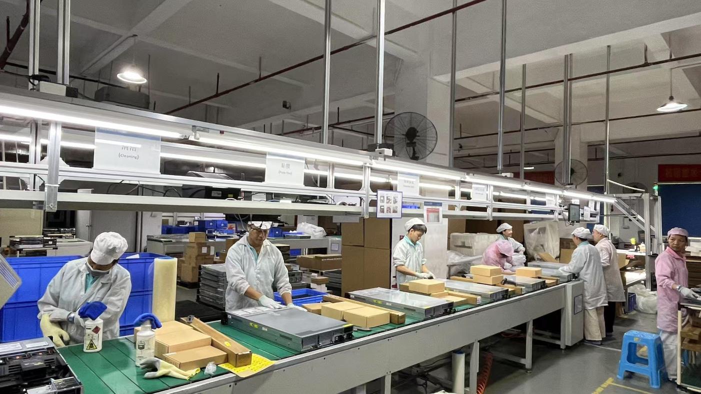
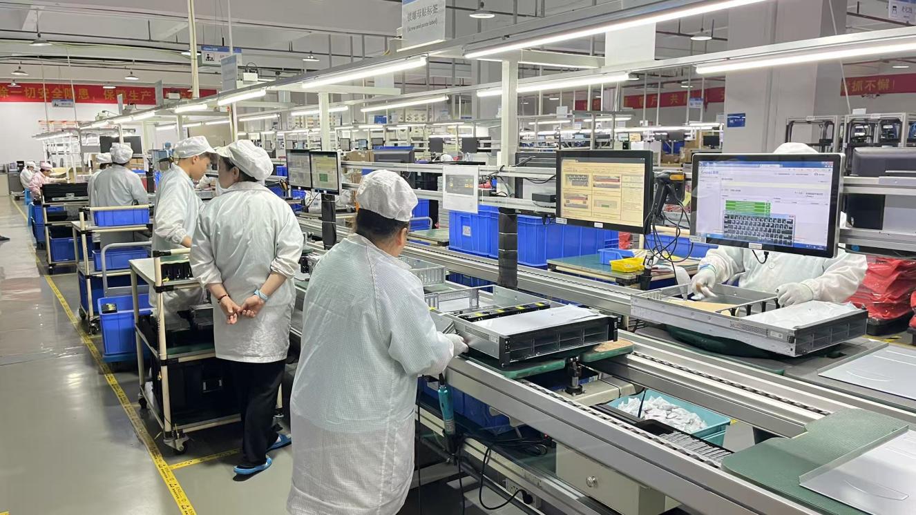
Operating a state-of-the-art 28,600 m² manufacturing facility, Celtrix integrates high-speed automated SMT lines, high-precision placement equipment, and multi-zone reflow profile management to guarantee defect-free solder joints. Our engineering capability centers on optimizing board layouts for high frequency, high thermal dissipation, and signal integrity—essential characteristics for server systems, high-power converters, and industrial automation assemblies.
Engineered for low signal loss, excellent thermal dissipation, and broad OS compatibility in enterprise networks.
A technical overview of layout engineering, solder chemistry, thermal management, and IPC quality classes for demanding electronics projects.
Modern PCBA manufacturing requires precise thermal profile management. To avoid thermal shock on fine-pitch components like 0201 passives and 0.4mm pitch BGAs, Celtrix implements a strict lead-free reflow process. We utilize high-grade SAC305 (Sn96.5Ag3.0Cu0.5) solder paste known for its exceptional mechanical strength and thermal fatigue resistance. Reflow zones are monitored via real-time profiling sensors, ensuring the soak zone remains between 150°C and 180°C to activate the flux, followed by a peak reflow temperature of 235°C to 245°C. The liquidus time is limited to 60-90 seconds to prevent intermetallic compound (IMC) layer overgrowth, which can cause brittle solder joints.
As clock speeds rise and components shrink, thermal management becomes a major bottleneck in PCB layouts. To address this, Celtrix integrates specialized material solutions, such as copper-aluminum composite cores, to construct thermal paths away from critical microchips. Through-hole plating (PTH) is optimized with thicker copper walls (minimum 25µm) to reduce thermal resistance. Heavy-copper PCBs (up to 4 oz copper weight) are regularly deployed for motor control, industrial welding machines, and automotive DC-DC converters, minimizing resistive losses and reducing heat buildup.
Different Korean industries require distinct manufacturing standards. In the Korean automotive sector (dominated by Tier-1 brands like Hyundai Mobis), assemblies must comply with the AEC-Q100 standard and IPC-A-610 Class 3 (High Reliability/Harsh Environment products). In contrast, the enterprise server and cloud computing sector in Incheon and Seoul demands multi-layer PCBs with low-loss dielectric constants to prevent signal attenuation at high bus speeds. In the heavy industrial sector of Ulsan and Busan, high-power PCBA designs (such as IGBT inverter driver boards and heavy-duty welders) focus on electrical clearance distances, moisture resistance, and conformal coating to protect against conductive dust and humidity.
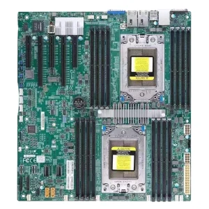
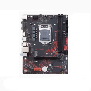
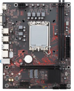
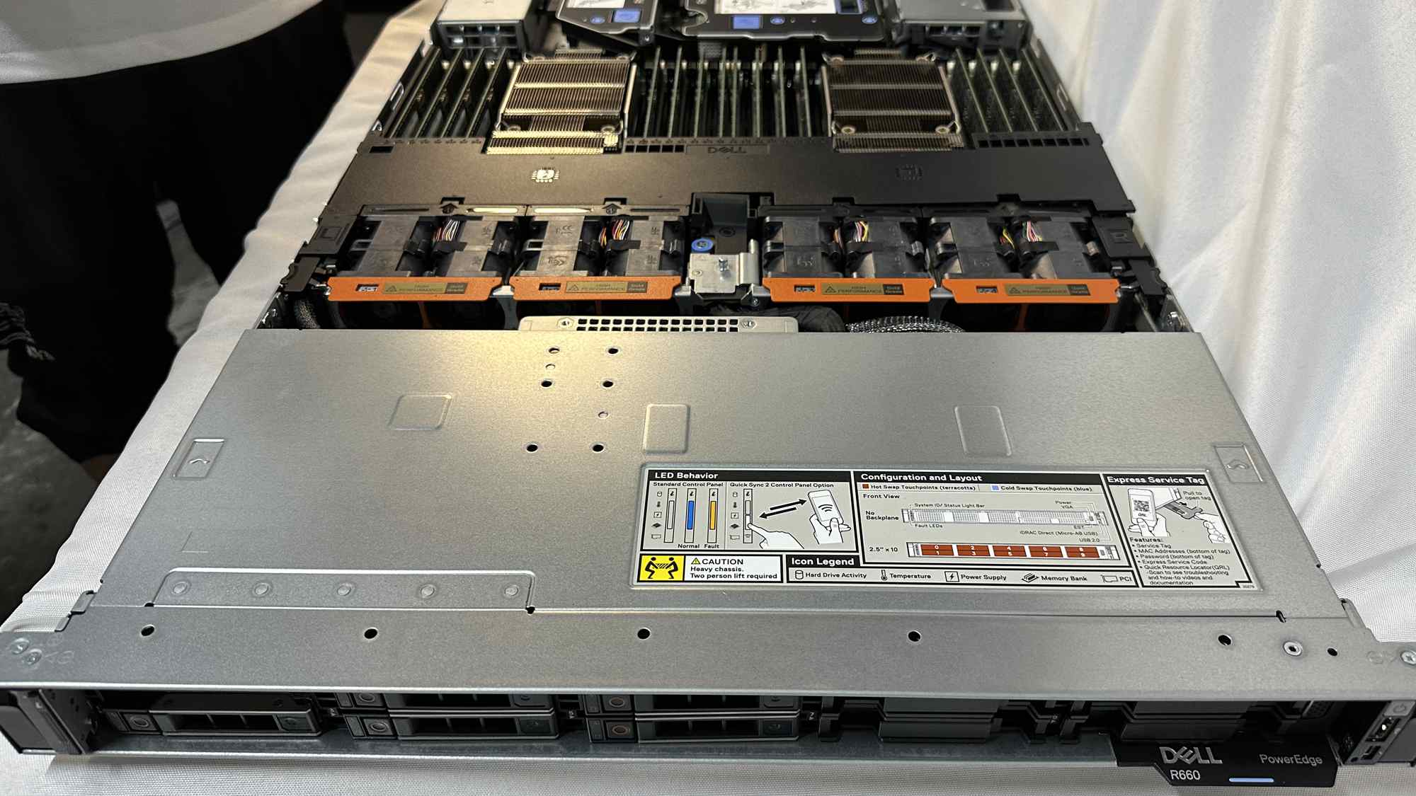
Comprehensive PCBA configurations supporting legacy interfaces, modern CPU architecture sockets, and heavy SMT component loads.
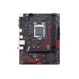
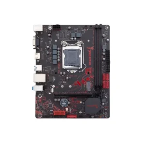
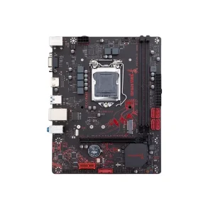
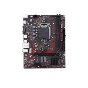
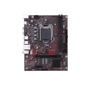
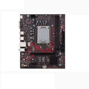
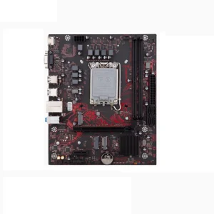
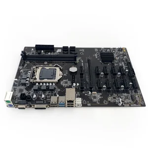
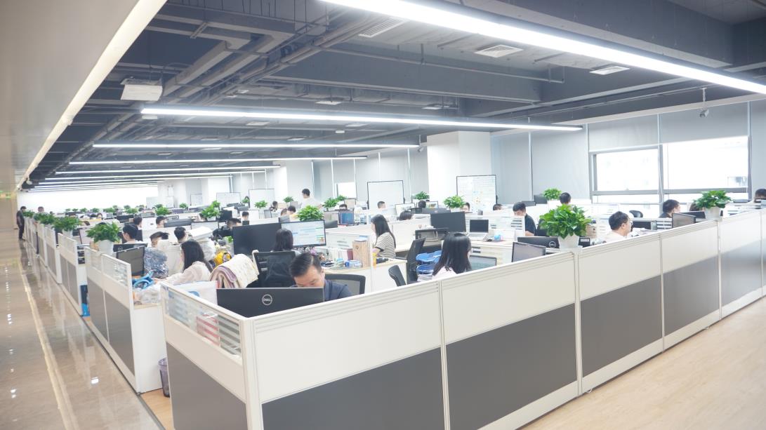
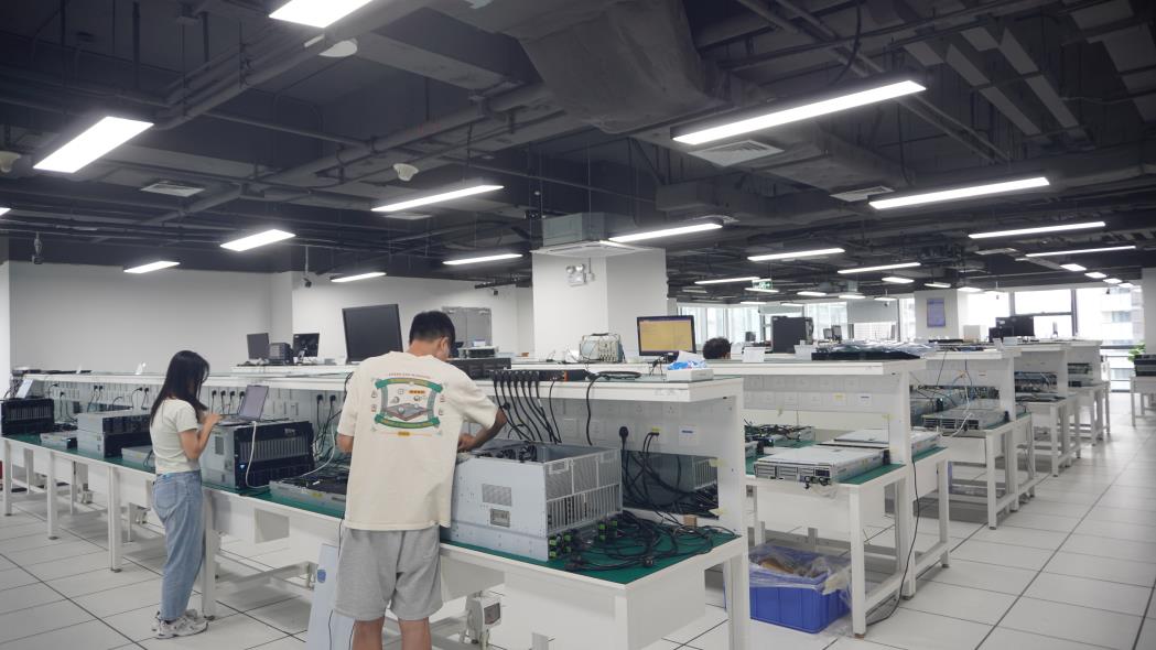
A visual tour of our production facility, showing our SMT assembly lines, testing chambers, and precision packing operations.
A strategic overview of environmental compliance, component sourcing resilience, and technological evolution in manufacturing.
The recent volatility in global semiconductor supply chains has highlight the need for robust traceability. Celtrix mitigates supply-chain risks by using an ERP-controlled Component Traceability System. Every batch of components—from passive MLCCs to main chipsets—is assigned a unique barcode linked to its manufacturer Certificate of Conformance (CoC). This tracking process helps prevent counterfeit parts from entering our supply chain, ensuring that every board assembled meets IPC-A-610 standards.
Routing data buses for DDR5 memory requires careful attention to trace layouts. DDR5 modules operate at speeds up to 6400 MT/s and above, where signal integrity is highly sensitive to trace lengths and impedance variations. Our R&D team utilizes advanced field solvers to analyze and minimize signal reflections, dielectric loss, and crosstalk on high-speed lines. By maintaining a strict 50-ohm single-ended and 90-ohm differential trace impedance layout, we ensure consistent signal transmission, even in dense multi-layer server mainboards.
Sustainable electronics manufacturing is no longer optional. Industrial buyers in Korea and Europe demand RoHS-3 and REACH compliance. Celtrix works closely with chemical suppliers to ensure all fluxes, cleaning agents, and conformal coatings are VOC-free or contain minimal volatile organic compounds. Our lead-free wave soldering and reflow processes use nitrogen inert atmospheres to reduce dross generation by up to 45%, minimizing scrap material and improving joint aesthetics.
Essential technical and trade questions answered by our engineering team for procurement managers and design engineers.
 Celtrix Memory