Advanced high-frequency modules and circuit assemblies engineered for Tokyo's leading power electronics and automotive sectors.
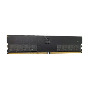
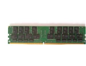
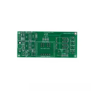
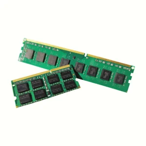
Tokyo stands as one of the world's most critical epicenters for industrial electronics design, precision engineering, and hardware prototyping. The metropolitan Tokyo area—encompassing research clusters in Shibaura, Ota City's precision manufacturing hubs, and neighboring Kanagawa high-tech belts—drives global standards in heavy-duty electronics. Specifically, the demand for Thick Copper PCBs (also widely known as heavy copper circuit boards with copper weight exceeding 3 oz/ft² up to 20 oz/ft²) has surged due to the rapid advancement of electric vehicles (EVs), industrial automation, smart power grids, and orbital transportation systems.
Within Ota-ku (Tokyo's historic industrial craftsmanship zone), specialized factories and technical consultants focus on design parameters that prevent thermal overload in high-current applications. While local Tokyo fabrication centers excel in rapid prototyping and high-mix, low-volume (HMLV) specialty designs, they face significant scaling bottlenecks when transitioned to commercial mass production. As a result, Tokyo’s engineering houses heavily rely on established global logistics partners to bridge the gap between high-precision local designs and cost-efficient, high-volume production facilities.
Tokyo's local design labs excel in creating ultra-precise layouts, incorporating complex thermal vias and heavy copper trace stack-ups.
With Japan's major automotive OEMs headquartered nearby, Tokyo acts as a core design testing ground for 800V EV power converter boards.
Heavy duty robotics manufacturers in Ota-ku deploy Thick Copper boards to control high-amp servo motors and industrial robotic arms.
Procuring Thick Copper PCBs involves balancing strict quality control with cost efficiency. While Japanese domestic manufacturing guarantees outstanding reliability, the high structural costs, limited scale, and longer lead times for raw copper sheets make domestic mass production economically challenging. Therefore, Tokyo's leading electronics suppliers and global procurement officers seek manufacturing partners in China that can match Japanese craftsmanship levels while offering vast production capacity, rapid lead times, and superior supply chain efficiency.
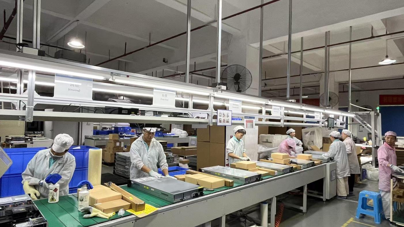
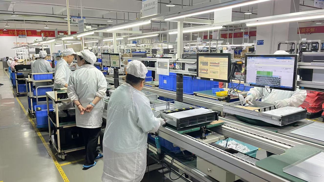
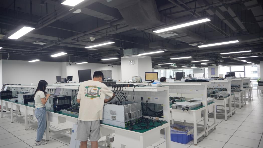
Celtrix Memory Technologies Co., Ltd. exemplifies this cross-border synergy. Operating with a massive 28,600 m² state-of-the-art production facility in China, Celtrix bridges the gap by providing rigorous quality control models—such as IQC, IPQC, AOI testing, and compatibility analysis—backed by 9 years of industry experience. This allows Tokyo-based system integrators to maintain their exact technical blueprints, while realizing the scale advantages of China's mature PCB laminating, copper plating, and manufacturing ecosystems.
| Parameter | Tokyo Domestic Fabrication | Chinese High-Efficiency Scale (e.g., Celtrix) | Synergized Procurement Model |
|---|---|---|---|
| Production Capacity | Limited to Low-Volume & Specialized Prototypes | Mass-Scale High-Volume Output (28,600 m² Facility) | Prototype in Tokyo, Mass Produce in China |
| Copper Plating Range | Mainly 2oz - 6oz standard runs | Up to 20oz Heavy & Extreme Copper Plating | Customized copper weight based on application |
| Lead Times | 4 to 8 weeks for specialized laminates | 10 to 15 business days (Rapid scaling) | Accelerated time-to-market for EV/Robotics |
| Quality Control Systems | Excellent, manual and micro-inspections | ISO 9001, automated AOI, FQC, and Burn-In | Dual-layered QA aligning with global standards |
Thick Copper PCBs are not general-purpose boards; they are specifically designed to carry heavy currents, withstand thermal stress, and protect critical components from electrical faults. In Tokyo's industrial and metropolitan sectors, these specialized boards are utilized in several high-demand environments:
As Tokyo transitions to green transportation, municipal zones are installing ultra-fast DC charging stations. Heavy copper boards (typically 4oz to 10oz) are used in power distribution units (PDUs) and high-power inverters, where heat dissipation is critical to prevent thermal runaway under continuous 150kW+ charging loads.
Tokyo's train networks require massive electrical loads. High-voltage power grids and transformer stations throughout JR East's Tokyo tracks rely on heavy copper layers to conduct thousands of amperes safely, preventing localized impedance and copper delamination under heavy vibration conditions.
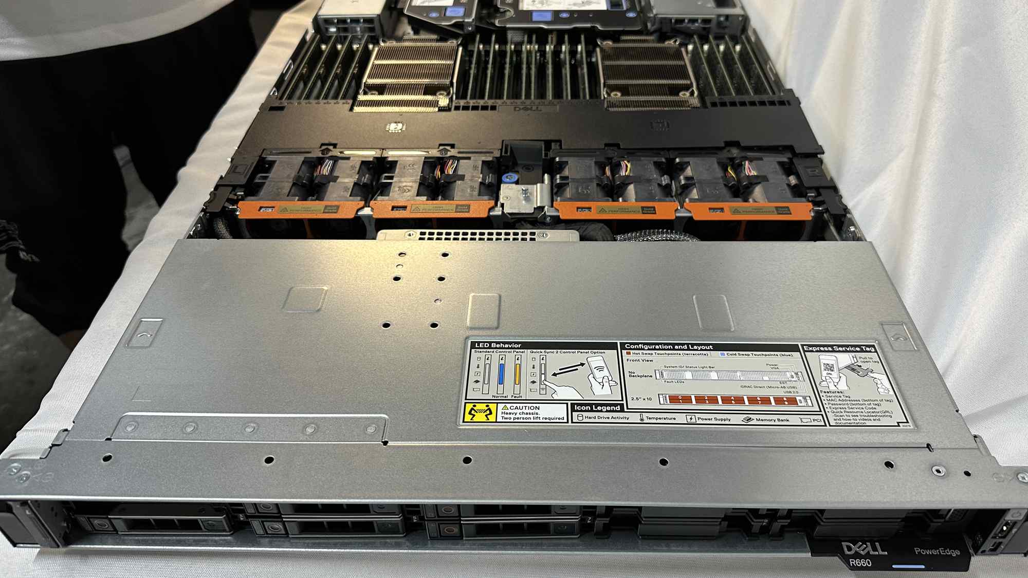
With data centers expanding in Tokyo Bay and Koto-ku to power next-generation generative AI workloads, server rack power supply units (PSUs) require extremely thick copper traces. These boards must deliver massive current to server motherboards while maintaining low electromagnetic interference (EMI) and a compact footprint.
Company Name: Celtrix Memory Technologies Co., Ltd.
Celtrix Memory Technologies Co., Ltd. is a professional DDR5 memory and high-performance hardware solution manufacturer dedicated to delivering premium hardware designs for global customers. Since its establishment in 2017, the company has focused on the research, development, manufacturing, and customization of premium memory products and high-density PCB integration for consumer, industrial, enterprise, and embedded applications.
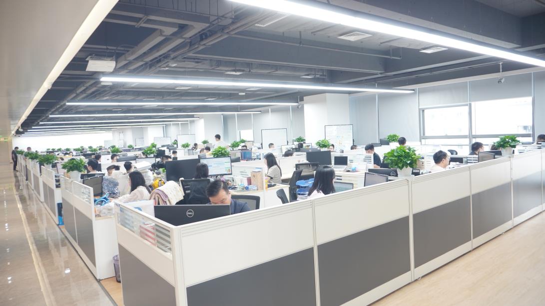
With a modern manufacturing facility covering 28,600 m², Celtrix integrates advanced production equipment, automated assembly lines, and strict quality management systems to ensure reliable product performance and consistent manufacturing standards. The company has accumulated 9 years of industry experience and 7 years of export experience, serving customers across more than 50 countries. Our annual export revenue exceeds USD 23 million, supported by an efficient global logistics network and responsive customer service.
Quality is the foundation of Celtrix. Every hardware component and high-density PCB module undergoes comprehensive inspections throughout the production process. Our quality control system is certified under ISO 9001 Quality Management System and involves:
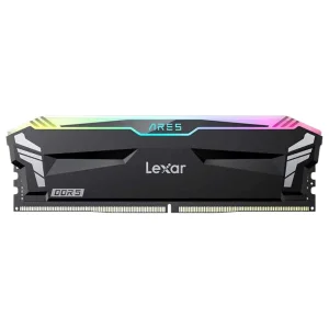
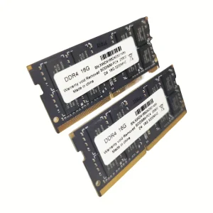
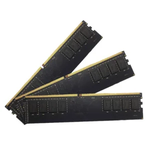
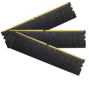
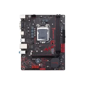
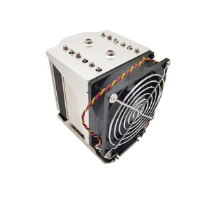
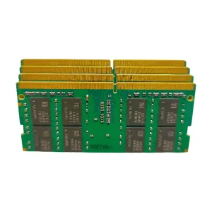
Browse our advanced DDR5/DDR4 high-performance modules and thermal components, designed for mission-critical enterprise systems and industrial computing architectures.
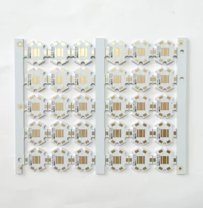
The global heavy copper PCB sector is experiencing dynamic technological transformations. As power density demands intensify, engineering teams must look beyond traditional manufacturing thresholds to maintain operational efficiency and safety. The following key trends are shaping the future of high-power electronics development:
While standard industry thick copper boards utilize 3oz to 8oz cladding, advanced research environments in Tokyo are increasingly requesting 20oz to 30oz copper structures. These "extreme copper" boards act as structural mechanical support and cooling sinks, integrating direct liquid-cooling interfaces within the substrate layer to handle intense localized currents.
To reduce overall circuit design complexity and costs, modern designers are turning to hybrid boards. These boards combine heavy copper layers for power distribution with standard-weight copper FR4 layers for high-speed logic control signals. Successfully executing these hybrid configurations requires specialized curing and thermal profiling, areas where Chinese factories with advanced SMT technology have demonstrated significant yields.
Environmental compliance regulations (such as RoHS and REACH) are forcing factories to transition toward halogen-free materials with high glass transition temperatures (Tg > 170°C). Under heavy current load cycles, these materials prevent resin cracking, trace lift-off, and material carbonization, extending the operating lifetime of industrial power control modules.
Answers to critical engineering and procurement questions regarding heavy copper designs, quality assurance, and manufacturing options.
A Thick Copper (or Heavy Copper) PCB features copper trace thicknesses ranging from 3 oz/ft² (105 µm) to over 20 oz/ft² (700 µm). Standard PCBs typically use 1 oz or 2 oz copper. Heavy copper boards are preferred in high-current and high-reliability environments because they minimize trace resistance, handle severe thermal stresses, and allow high-power components to be integrated directly onto a single board.
Celtrix operates under strict ISO 9001 quality guidelines. Every batch undergoes a series of inspections including Incoming Material Inspection (IQC), In-Process Quality Control (IPQC), Automated Optical Inspection (AOI) for trace accuracy, functional load tests, burn-in testing, and compatibility inspections. This meticulous protocol has enabled our products to meet strict international standards across 50+ export destinations.
Tokyo design centers provide unparalleled initial prototyping, but scaling to volume runs locally is often restricted by high energy costs, space constraints, and limited heavy copper raw material networks. Partnering with a Chinese manufacturer like Celtrix allows companies to leverage state-of-the-art 28,600 m² factories, rapid automated production lines, and robust raw copper supply chains, reducing costs and lead times while maintaining Japanese quality expectations.
Effective thermal management involves integrating thermal vias, utilizing thick aluminum or copper metal substrates, and designing wide, heavy-gauge copper paths. These paths efficiently pull heat away from active semiconductors, distributing it across the outer metal surfaces or conductive casing, which reduces the reliance on external cooling fans.
Celtrix offers extensive OEM/ODM support, including customized logo printing, specific PCB layer stack-ups, targeted capacity and SPD programming for memory modules, customized heat sink shapes, label placement, and individual private-label retail packaging options.
Standard industrial PCB orders are typically fabricated, tested, and dispatched within 10 to 15 business days. Highly complex hybrid structures or extreme thickness layers (e.g., >12 oz) may require slightly longer to ensure optimal plating density and curing parameters.
 Celtrix Memory