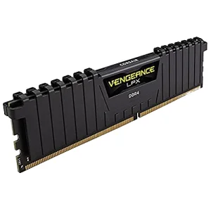
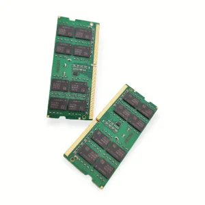
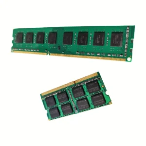
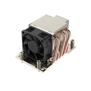
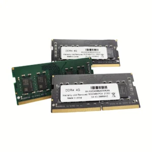
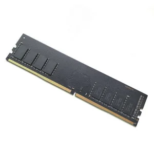
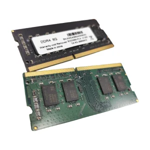
Engineered for mission-critical operations. Discover our advanced memory architecture and RF substrate products designed to work in synergy with heavy copper power distribution networks.
Deep-dive research into how heavy copper electronics are accelerating Britain's electrification, defense, and power grid modernization.
The United Kingdom's commitment to achieving Net-Zero greenhouse gas emissions by 2050 has sparked an unprecedented demand for robust power electronics. Central to this transition is the reliance on Thick Copper PCBs (defined as boards with copper weight exceeding 3 oz/ft² up to 20 oz/ft² or more). From renewable energy generation in the North Sea wind turbines to EV fast-charging stations across England's highway networks, heavy copper circuits provide the required electrical and thermal performance limits that standard FR4 boards cannot sustain.
UK aerospace and defense hubs in the South West and Midlands demand high-reliability electronics capable of withstanding extreme vibration and thermal cycling. Thick copper PCBs serve as reliable structural cores and heat sinks, eliminating failures in radar, avionics, and marine navigation systems.
"Standard PCBs often fail when handling high-current thermal loads. The adoption of thick copper (3oz - 15oz) has become the gold standard for UK system integrators seeking to eliminate active cooling mechanisms, reduce weight, and lower overall enclosure sizes."
UK rapid-chargers require high voltage (800V+) and high current density. Heavy copper tracks minimize I²R losses, preventing thermal degradation and ensuring lifetime reliability in wet coastal climates.
In offshore wind farms and utility-scale solar arrays in Wales and Scotland, thick copper substrates distribute massive currents from raw generator output to grid-tied converters, acting as integrated busbars.
To power London's growing financial data centers and automated warehouses in the Midlands, heavy-duty power supplies require thick copper multi-layer boards to support compact, high-frequency switching regulators.
Combining world-class high-speed logic module design with heavy-duty structural electronics capability.
Celtrix Memory Technologies Co., Ltd. is a professional manufacturer and exporter dedicated to delivering high-performance DRAM solutions, advanced PCBs, and system assemblies for global customers. Since our establishment in 2017, we have focused on the research, development, manufacturing, and customization of premium hardware for consumer, industrial, enterprise, and embedded applications.
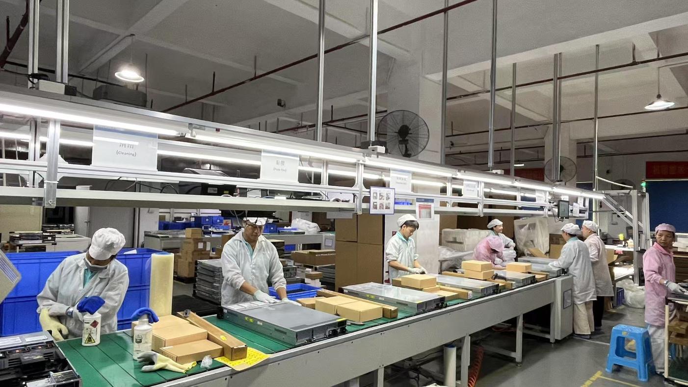
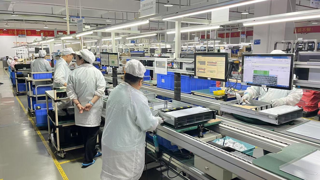
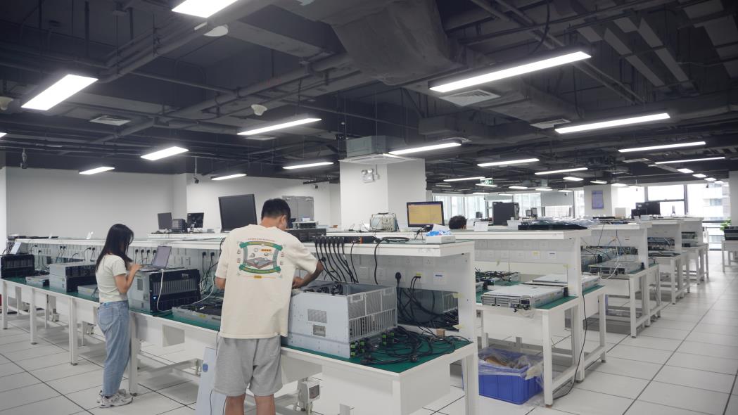
Equipped with a modern manufacturing facility covering 28,600 m², Celtrix integrates state-of-the-art production lines, automated high-precision assembly, and strict quality control workflows. This ensures reliable performance in high-stress thermal and electrical environments.
With 9 years of industry experience and 7 years of export history, we support system integrators and distributors across more than 50 countries, including the United Kingdom, delivering customized configurations, quick-turn prototyping, and bulk production services.
| Celtrix Corporate Profile at a Glance | |
|---|---|
| Year Established | 2017 (9 Years Industry Heritage) |
| Factory Footprint | 28,600 m² Modern Smart Facility |
| Export Reach | 7 Years Serving 50+ Countries (Including UK) |
| Annual Export Revenue | USD 23 Million+ |
| Quality Standards | ISO 9001, IQC/IPQC/AOI/FQC Workflows |
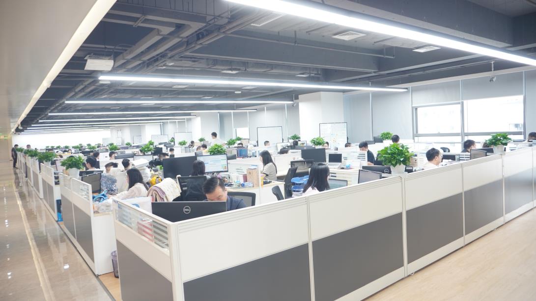
| R&D Workforce | 142 Dedicated Engineers |
| Annual Product Releases | 168 New Design Configurations Released |
Understanding the strict tolerance and processing parameters required for high-yield heavy copper production.
Fabricating PCBs with thick copper layers (ranging from 3oz up to 20oz) presents unique challenges. The primary obstacle is the etching process, which requires precise control to prevent undercut and trace narrowing. High-viscosity resin formulas and advanced thermal lamination cycles are critical to eliminate voids in the dielectric between the thick copper tracks.
| Technical Characteristic | Standard PCB Range | Heavy Copper Range | Extreme Copper Range |
|---|---|---|---|
| Copper Foil Weight | 0.5 oz - 2 oz / ft² | 3 oz - 8 oz / ft² | 9 oz - 20+ oz / ft² |
| Outer Trace Width / Space (Min) | 4 mil / 4 mil | 8 mil / 10 mil (Depends on oz) | 15 mil / 20 mil (Depends on oz) |
| Lamination / Prepreg System | Standard Epoxy (FR4) | High-Tg FR4 (Tg170/180) / Rogers | Polyimide / Custom High-Thermal Resins |
| Solder Mask Clearance | 2 mil | 5 mil | 8+ mil (High vertical wall build-up) |
| Maximum Current Carrying Capacity | < 20 Amperes | 20 - 150 Amperes | 150 - 500+ Amperes |
| Primary Application Areas | Logic Gates, Microcontrollers | Power Supplies, Rectifiers, Inverters | Automotive Traction, Smart Grid Inverters |
As a global OEM provider, Celtrix bridges the cost and speed advantages of China's advanced component supply chain with the rigorous compliance requirements of the British electronics industry. Every shipment destined for the UK conforms to UKCA (UK Conformity Assessed) guidelines, RoHS, and REACH regulations. By utilizing automated optical inspection (AOI) alongside rigorous thermal shock chamber testing, we ensure that the boards we manufacture transition smoothly into local assembly lines in locations such as Bristol, Leeds, and Belfast.
Get answers to common design, engineering, and logistics questions from our advanced technical team.
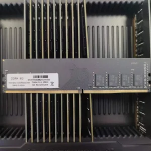
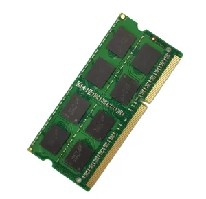
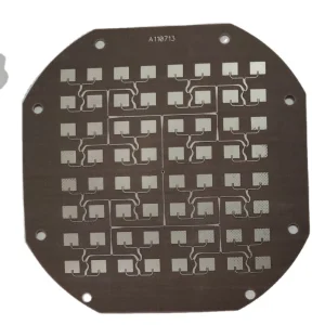
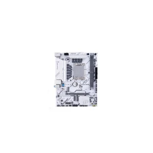
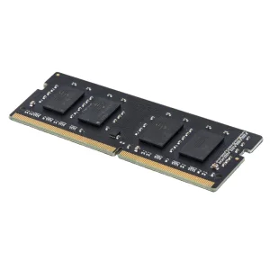
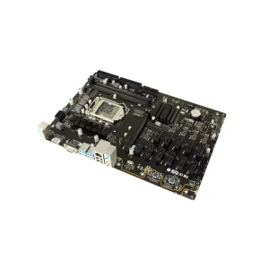
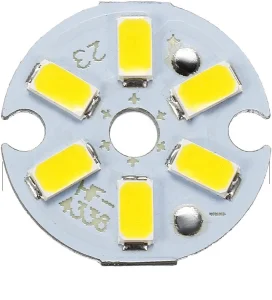
Explore our integrated portfolio of high-density memory modules, motherboards, coolers, and high-frequency PCBs.
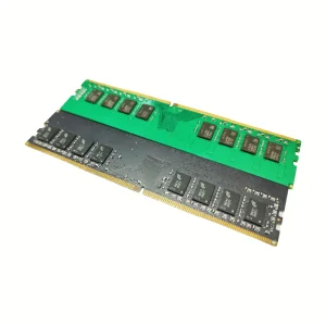
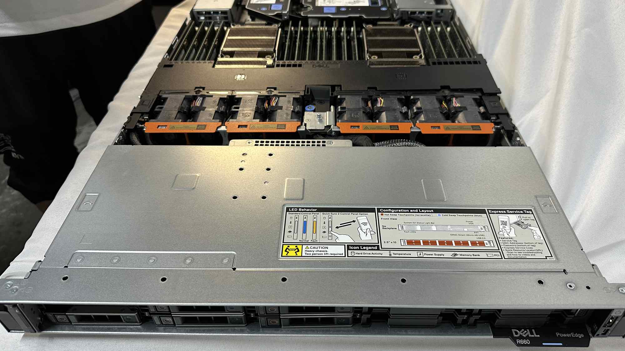
A closer look inside our production facilities, clean rooms, and quality control departments.
Connect with our expert R&D engineering department. Get comprehensive design review, material selection guidance, and a detailed DFM analysis for your next release.
Send Inquiry Now Celtrix Memory