Celtrix Memory
1 / 5
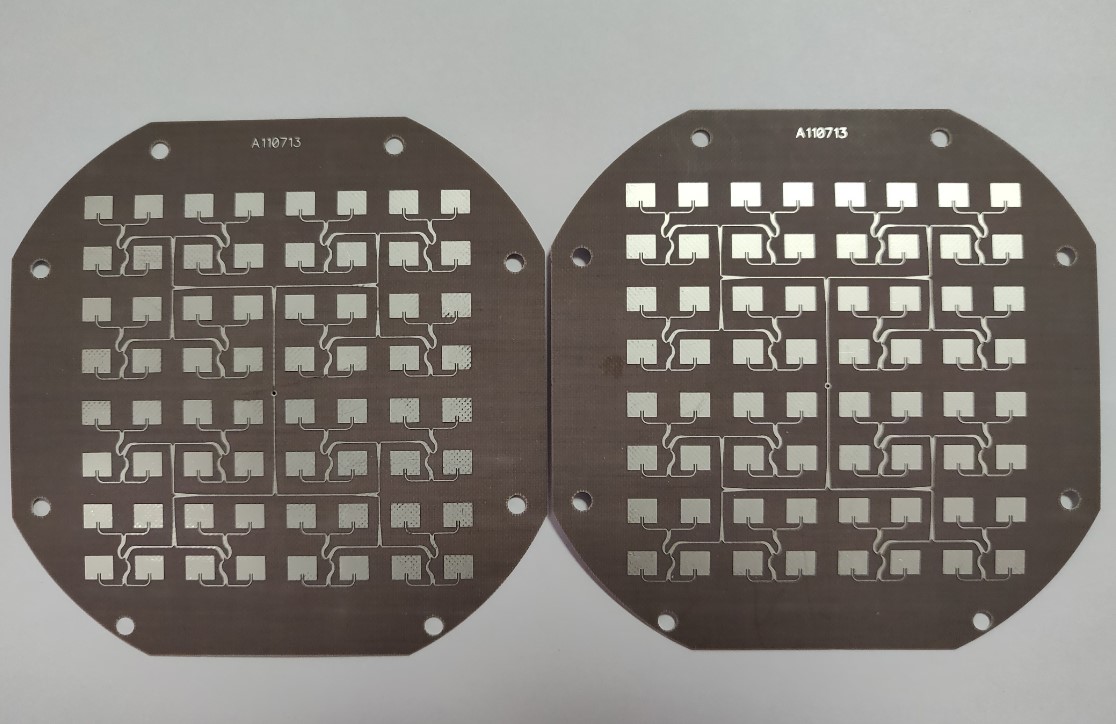
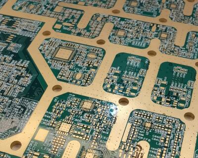
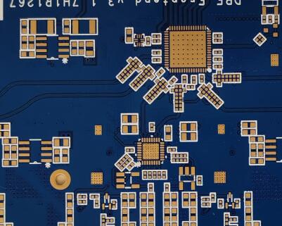
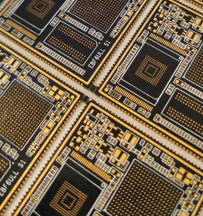
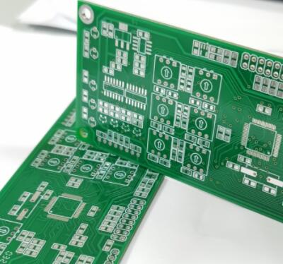
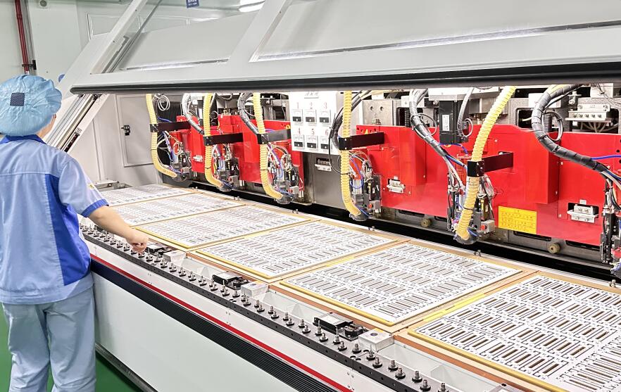
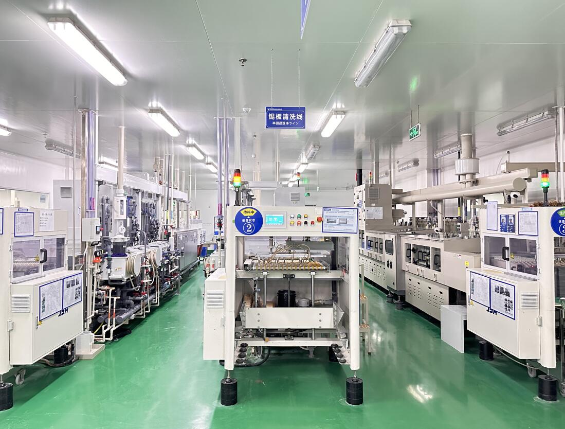
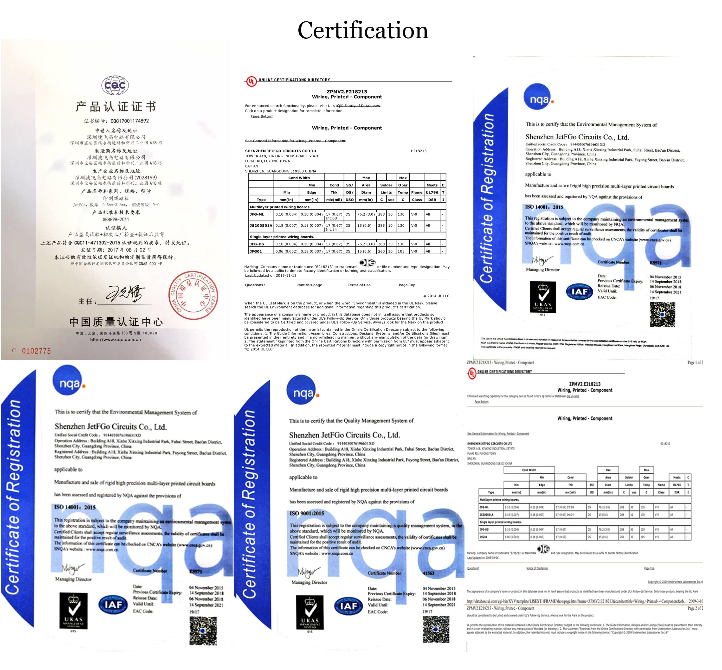
We are a leading manufacturer specializing in high-density multilayer printed circuit boards and specialty boards. With certifications including UL, ISO9001:2015, ISO14001:2015, CQC, IATF16949:2016, and "National Military Standard," we provide top-quality products and services. Our extensive product range includes multilayer boards, impedance boards, high-frequency boards, high TG thick copper foil boards, 5G high-speed boards, buried blind via boards, aluminum-based boards, hybrid dielectric boards, HDI, rigid-flex boards, specialty boards, and customized solutions.
Driven by technological innovation, our products are widely used in industries such as communication equipment, industrial control, automotive electronics, energy and power, medical devices, IoT, research institutions, aerospace, and defense. With over 19 years of experience, we have served over 1,000 technology innovation-oriented enterprises with rapid prototyping and mass production services. We are committed to delivering cutting-edge solutions and exceeding customer expectations in the dynamic electronics industry.
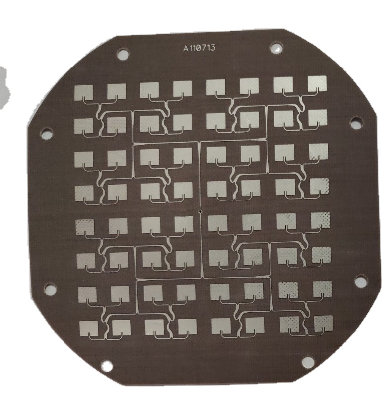
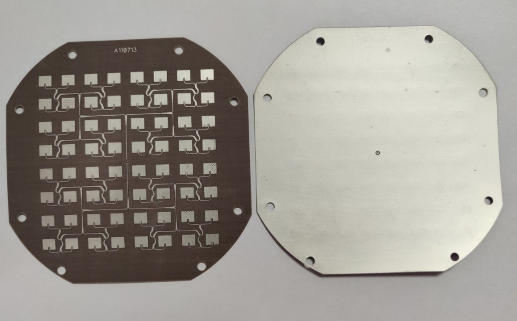
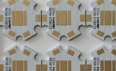
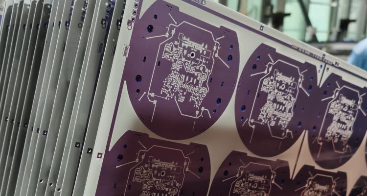
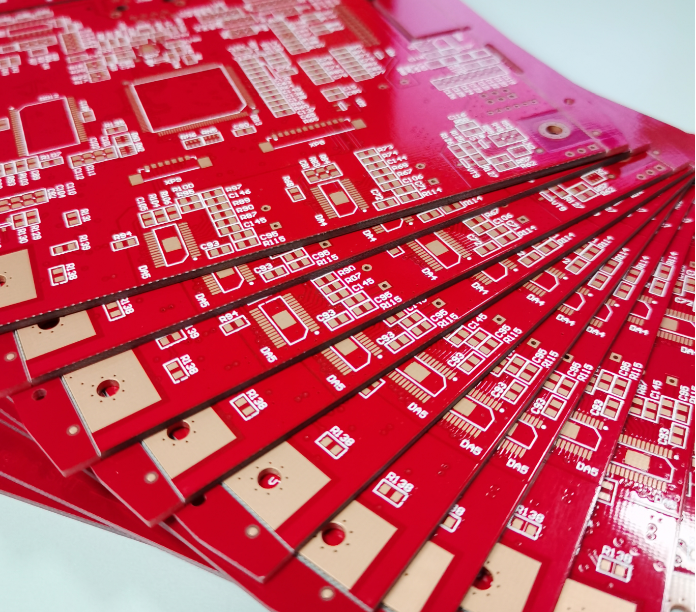
| Model | Aluminum substrate |
|---|---|
| Solder mask coverage | Resin plug hole |
| Outer copper thickness | 0.5oz |
| Forming method | Mold Forming |
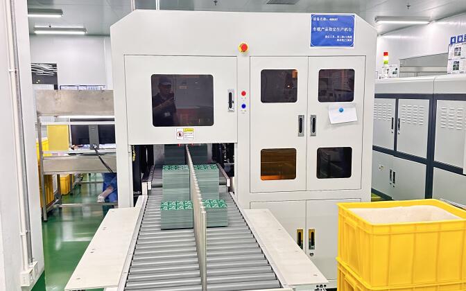
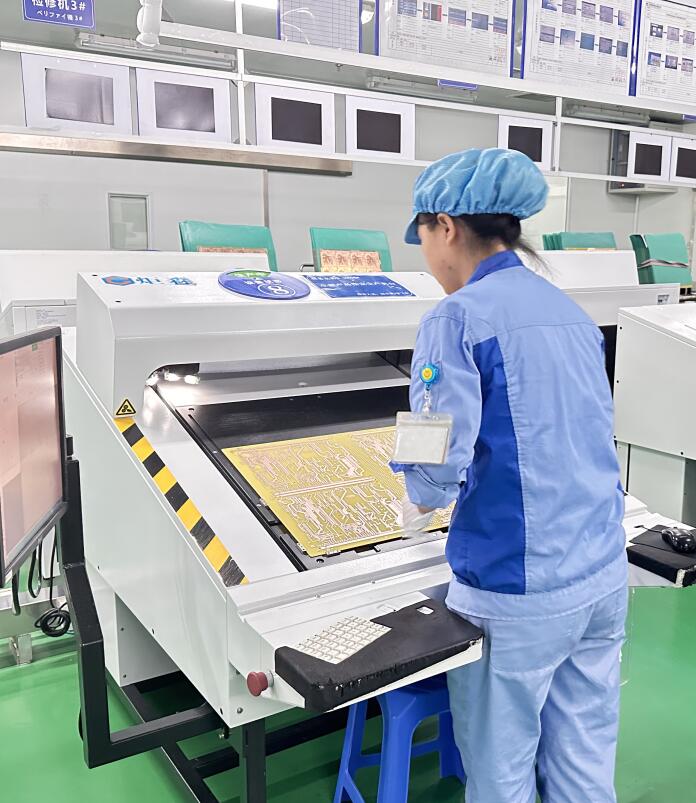
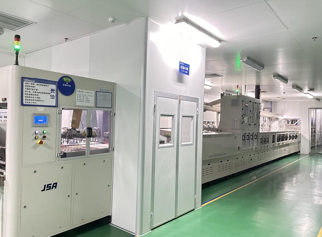
| Category | Volume Production | Sample Processing |
|---|---|---|
| Layer count | 1-68L | 64 Layer |
| Max thickness | 10mm (394mil) | 14mm (551mil) |
| Min line width/space (Inner) | 2.2mil/2.2mil | 2.0mil/2.0mil |
| Min line width/space (Outer) | 2.5mil/2.5mil | 2.2mil/2.2mil |
| Alignment with the core board | ±25um | ±20um |
| Inner layer alignment | ±5mil | ±4mil |
| Max copper | 6Oz | 30 oz |
| Holes size (Mechanical drilling) | ≥0.15mm (6mil) | ≥0.1mm (4mil) |
| Holes size (Laser drilling) | 0.1mm (4mil) | 0.050mm (2mil) |
| Max unit size | 850mm x 570mm | 1000mm x 600mm |
| Max panel size | 1250mm x 570mm | 1320mm x 600mm |
| Aspect ratio (Unit) | 20:1 | 28:1 |
| Aspect ratio (Panel) | 25:1 | 35:1 |
| Lead-free/Halogen-free materials | EM827, 370HR, S1000-2, IT180A, EM825, IT158, S1000 / S1155, R1566W, EM285, TU862HF | |
| High-speed PCB material | Megtron6, Megtron4, Megtron7, TU872SLK, FR408HR, N4000-13 Series, MW4000, MW2000, TU933 | |
| High-frequency PCB material | Ro3003, Ro3006, Ro4350B, Ro4360G2, Ro4835, CLTE, Genclad, RF35, FastRise27 | |
| Other Materials | Polyimide, Tk, LCP, BT, C-ply, Fradflex, Omega, ZBC2000 | |
| Surface finished | HAL, HAL-LF, ENIG, IMMERSION TIN, OSP, IMMERSION SILVER, GOLD FINGER, Hard Gold/Soft Gold Plating | |
| Special technology | Blind & buried holes, Via in pad, Semi-plating holes, Counterbore, Step mounting holes, drill Mixed RF PCB, Busbar PCB | |

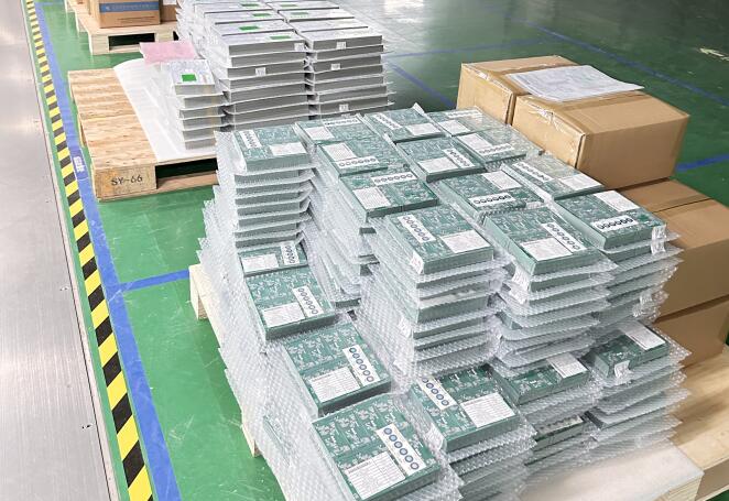
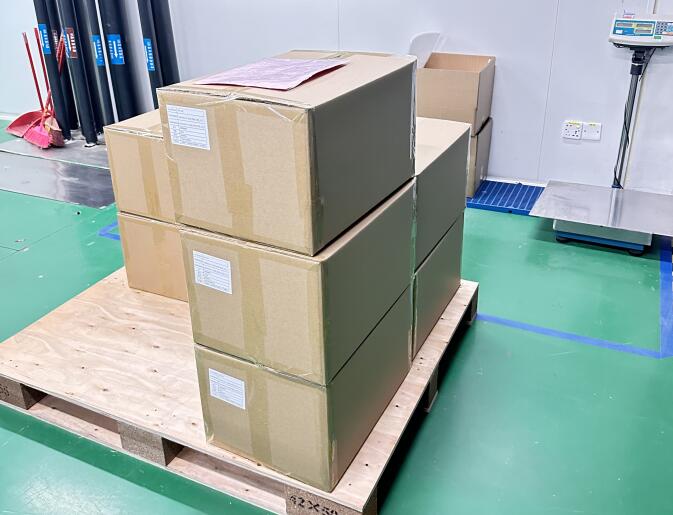
We ship PCB orders globally with the following reliable options:
| Layer | Sample Shortest Lead Time | Sample Standard Lead Time | Mass Production Lead Time |
|---|---|---|---|
| 2 layer | 24 h | 3 days | 6-7 days |
| 4 layer | 36 h | 5 days | 8-10 days |
| 6 layer | 48 h | 5 days | 8-12 days |
| 8 layer | 72 h | 5 days | 9-12 days |
| 10 layer | 4 days | 7 days | 14 days |
| 12 layer | 4 days | 7 days | 16 days |
| 14 layer | 5 days | 8 days | 16 days |
| 16 layer | 5 days | 9 days | 18 days |
| 18 layer | 7 days | 10 days | 18 days |
| 20 layer and above | To be negotiated | To be negotiated | To be negotiated |
24h technical support, 24h Gerber files handling. Complete EQ within 4-8 hours. Support for 400 new project engineering reviews.
RS-274-X, RS-274-D, CAD, DXP, Protel 99 SE, PADS, and GC-CAM.
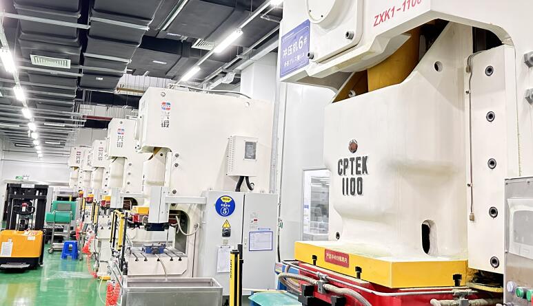
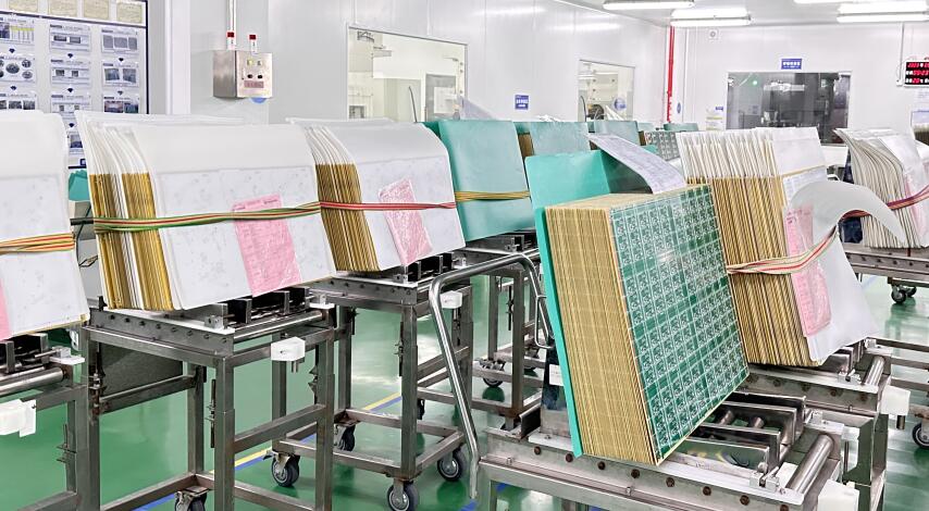
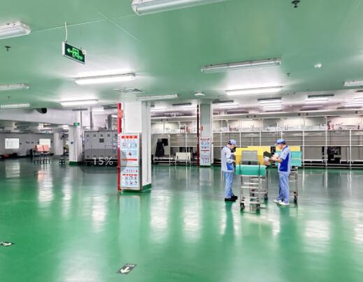
All processes running 24 hours. Monthly capacity of more than 10K high mix part numbers in production. Over 100 QTA orders processed daily. One-step service from prototype to mass production.
24 hours quick response for inquiries. 4 hours quick response for quotation services.
A1: We can manufacture up to 64 layers for standard sample processing, and from 1 to 68 layers for standard mass volume production.
A2: We work with high-quality industry materials including Rogers (Ro3003, Ro3006, Ro4350B, etc.), Megtron4/6/7, Teflon (Tk), LCP, BT, and high TG halogen-free materials.
A3: We accept RS-274-X, RS-274-D, CAD, DXP, Protel 99 SE, PADS, and GC-CAM file formats.
A4: Our shortest lead times are 24 hours for 2-layer boards, 36 hours for 4-layer boards, and 48 hours for 6-layer boards.
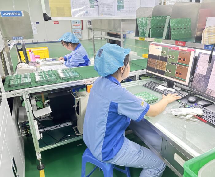
A5: Our quality processes are strictly certified to ISO 9001:2015, ISO 14001:2015, IATF 16949:2016, UL, CQC, RoHS, and Reach standards.
A6: We offer global express air shipping (UPS, DHL, TNT, CTS, FEDEX), railway shipping, seaborne shipping, and customer-designated logistics methods.