Celtrix Memory
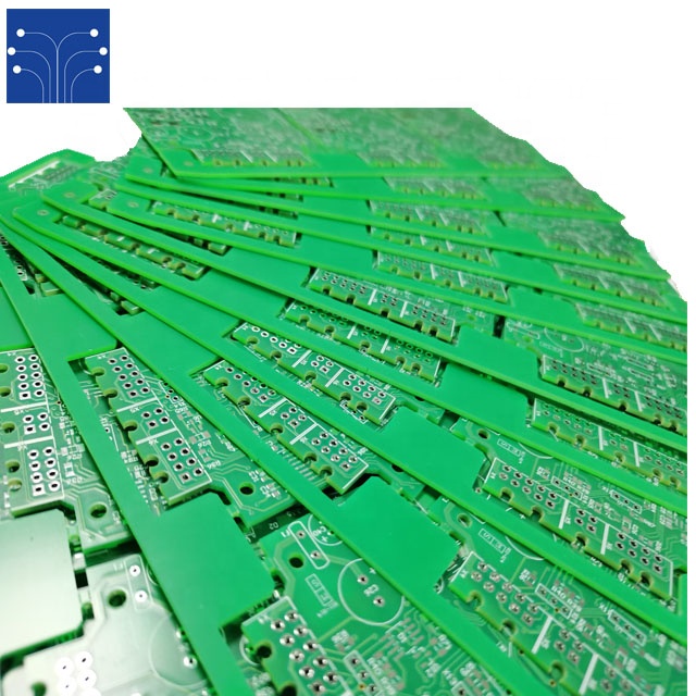
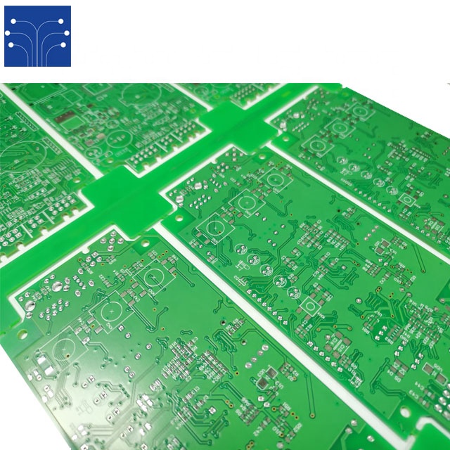
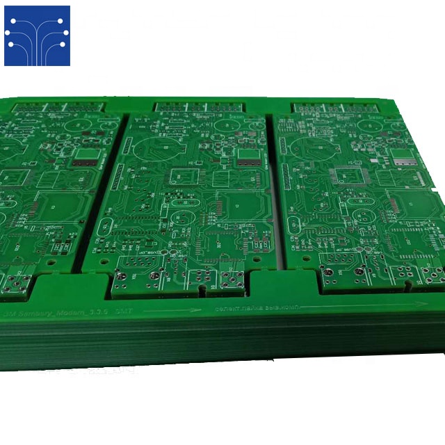
1 / 5

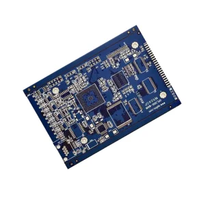
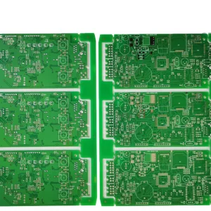
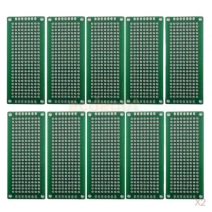
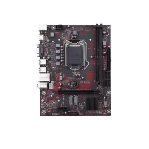
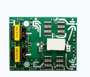
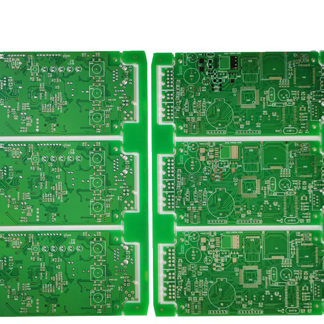
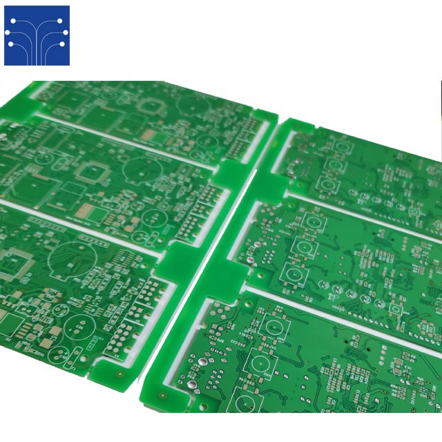
Our facility has invested in the best equipment, environment, and staff training. We have production capability for standard and HDI, Rigid, RF, and high-frequency PCBs, together with through-hole and min 0201 chips, 0.2mm pitch BGA balls SMD soldering, in small batch, mid-volume, and high-volume quantities.
Professional PCB electronics manufacture services, where every PCB enquiry or order is handled in the strictest confidence. We can fabricate Laser holes, Impedance Control PCB, Buried & Blind Holes PCB, Countersunk holes, and other special material or special process PCBs.
TOP PCB High frequency - Microwave Circuits Roger 4000+ FR4 Mixed Pressure
| Items | Capacity |
|---|---|
| 1. Base Material | Roger 4000+ FR4 Mixed pressure |
| 2. Layer / PCB thickness | 6 Layer / 1.6mm |
| 3. Copper thickness | 1oz copper |
| 4. Solder mask / Silkscreen | Green solder mask / White silkscreen |
| 5. Surface finished | Immersion gold |
| 6. Min width/space | 4.5 / 3.5 mil |
| 7. Min holes | 0.2mm |
| 8. Technics Characteristic | Trace width ± 10 % |
| 9. Technical Requirement | Process difficulty: Roger 4000+ FR4 Mixed pressure, IPC class II standard. |
| Standard Produce time | 9-12 days |
| Fast produce time | 24h ~ 90h |
| Payment and shipment |
1) By T/T bank (wire transfer, the most popular way) 2) By Western Union 3) By Paypal (especially for samples) 4) By Cash |
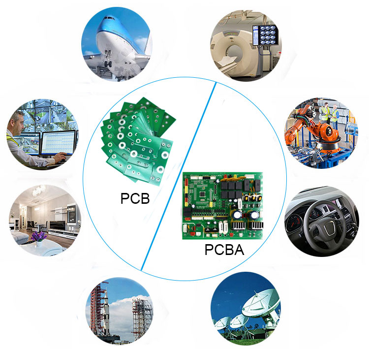
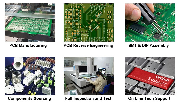
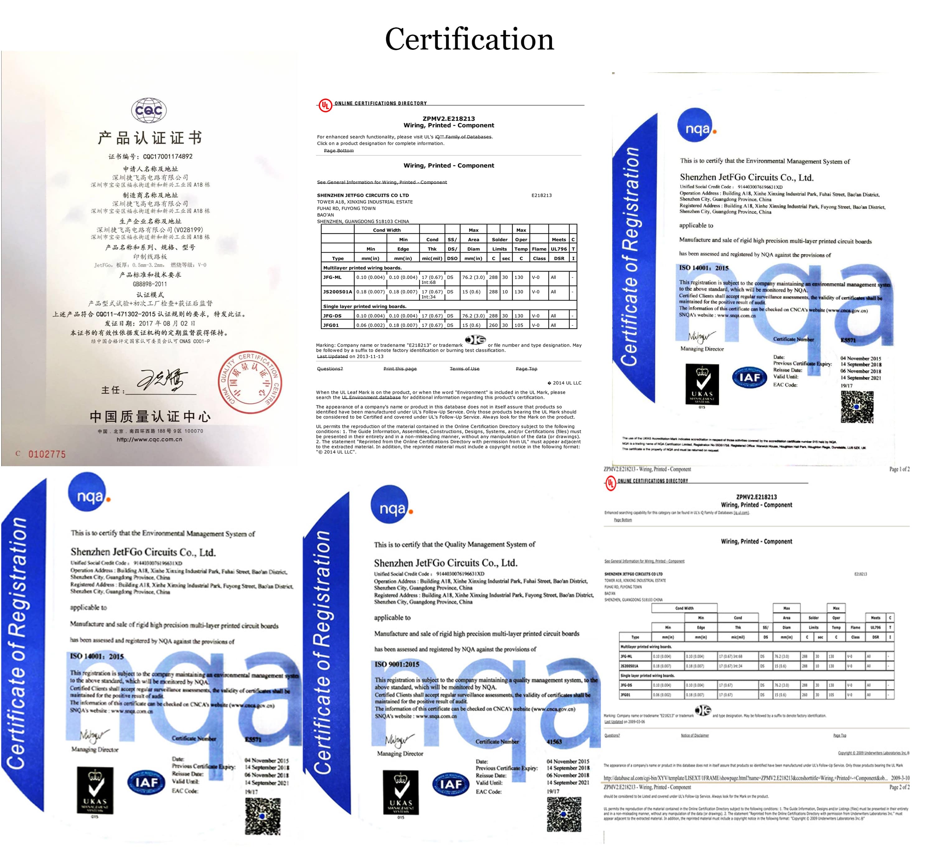
We have established a quality system with ISO9001 and strictly implement the IPC class III standard to inspect quality. 100% inspection includes electrical test and AOI inspection. We carry out high voltage tests, impedance tests, microsection analysis, weldability tests, and other professional testing procedures to keep up with the high demands of high-tech products.
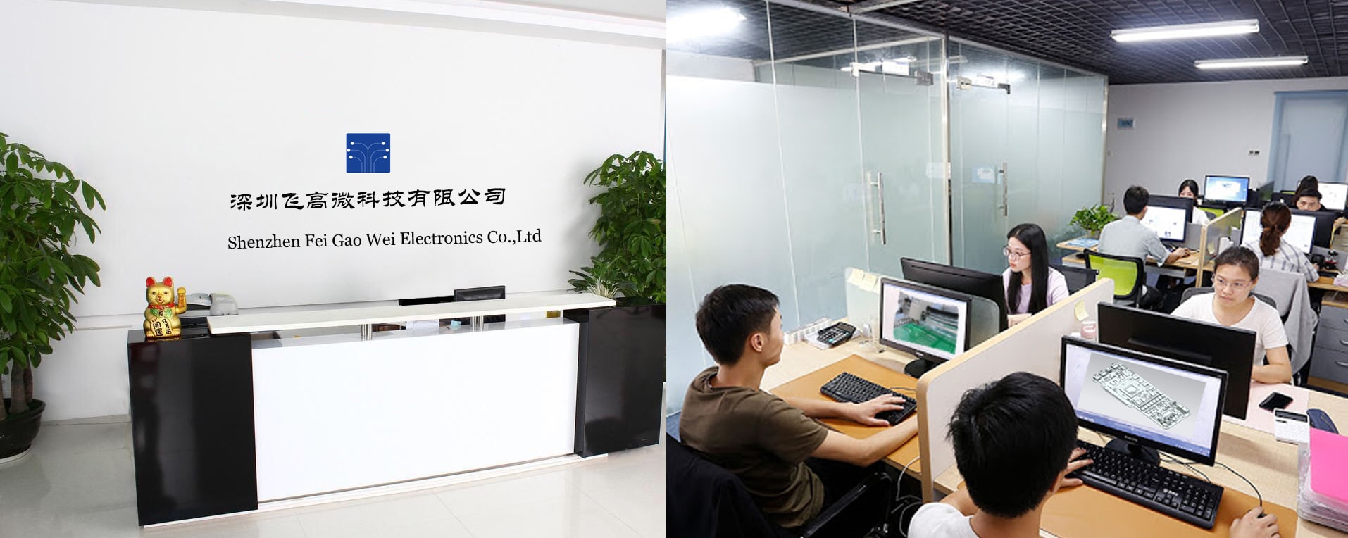
We have been manufacturing printed circuit boards for more than 20 years. Established in 1990, we serve as a competitive, high-tolerance, high-quality PCB manufacturer for small, medium, and large production quantities. Whether you require a prototype printed circuit board assembly or large-volume production, we have the capacity and expertise to satisfy all requirements.
We pride ourselves on offering professional services with a friendly approach where quality remains paramount, in full accordance with our ISO9001 Quality Management system and UL Approval.
Specializing in Quick-turn PCB services, we offer an industry-leading turnaround time as fast as 24 hours. When your business needs rapid PCB prototyping, you can count on us to deliver high-quality printed circuit boards on time and at competitive prices.
We encourage prospective clients to visit our facilities. We maintain an open-door policy for all customers, both new and old. Once you see our facility and consult with our expert staff, you will find total confidence in our ability to meet your specific needs.
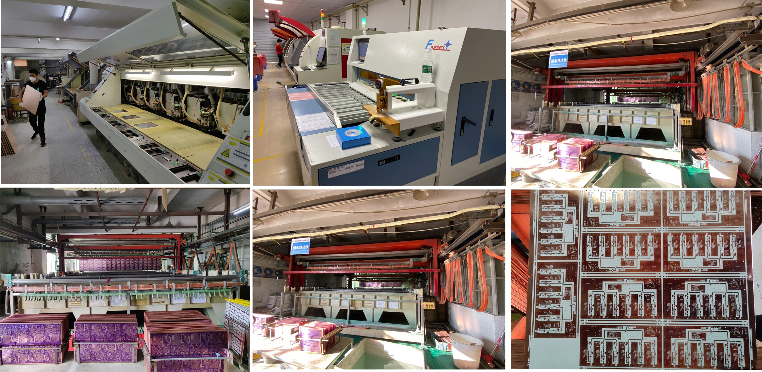
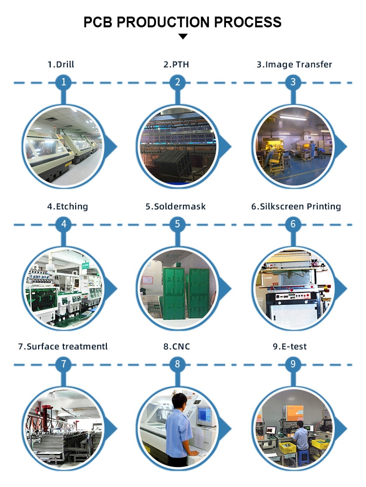
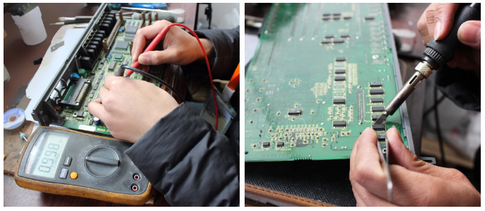
We have over 15 professional engineers, and all products are fully tested before warehousing and shipping.
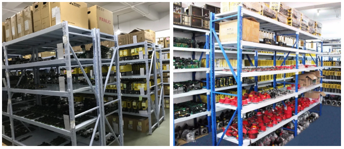
We maintain a large stock of parts and products. When you need to purchase or repair parts, it is our pleasure to serve you and build a reliable business partnership.
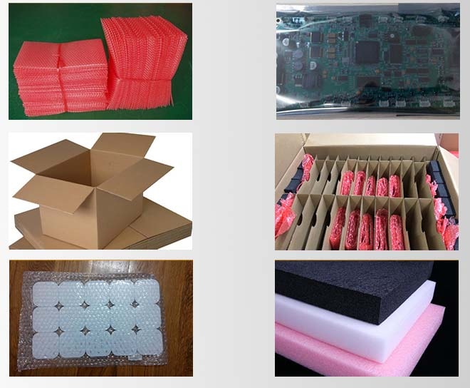
We prioritize giving our customers high-quality products while maintaining a secure and complete packaging system. We provide personalized packaging services tailored to every order.
Common packaging:
PCB: Sealed bag, Anti-static bags, Suitable carton.
PCBA: Antistatic foam bags, Anti-static bags, Suitable carton.
Customized Cartons:
External cartons can be printed and customized according to specific customer requirements, marks, destinations, and other information.

We provide one-stop PCB/PCBA customization services to meet all customer requirements.
To offer high-quality PCB/PCBA, we perform strict quality assurance processes:
1. How can you guarantee the quality of the parts?
We offer a 3-month warranty for used parts and a 1-year warranty for new parts. If parts do not function correctly upon arrival, you can return them to us within 7 days, and we will cover the return shipping costs.
2. How are the products packaged for shipping?
We use 3cm thick foam board to fill and protect the inside of the box. Parts are generally packed in cartons. If they are excessively heavy, we will construct a custom wooden box to ensure safe transit.
3. What payment methods and express shipping options are accepted?
We accept main payment methods including Paypal, Western Union, and T/T (Bank Transfer). For shipping, we utilize major courier services such as UPS, EMS, TNT, FEDEX, and DHL.
4. Do you test the parts, and what is your lead time?
Yes, we have complete testing equipment, and all parts are 100% tested before shipment. Lead times depend on the specific requirements, but we have items in stock that can ship in 1-2 days, while custom projects take 9-12 days.
5. Can you produce PCBs from a physical sample instead of a Gerber file?
Yes, we can copy files based directly on your physical sample to generate the Gerber files required for production. Additionally, we can design Gerber files if you provide the schematic diagrams.
6. Are my design files kept safe and confidential?
Absolutely. All customer design files are kept strictly confidential inside our facility and are never shared with third parties. We are fully prepared to sign a Non-Disclosure Agreement (NDA) to secure your intellectual property.