Direct access to our advanced high-frequency substrates, high-speed computer memory interfaces, and complex multi-layer PCB components engineered for extreme environments.

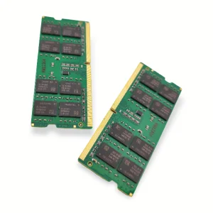
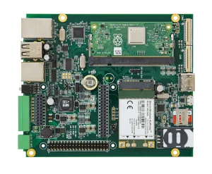
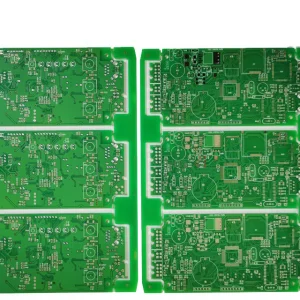
In the era of hyper-scale computation, satellite data relay, and 5G/6G communication infrastructure, the demand for High-Frequency Circuit Boards (HFCBs) has reached unprecedented levels. As industrial designs transition from legacy megahertz applications to high-gigahertz domains, signal attenuation, propagation delay, and thermal dissipation have become critical engineering challenges. Standard FR-4 substrates fall short when managing insertion loss, signal dispersion, and dielectric stability above 10 GHz. Modern electronics require highly optimized high-frequency laminates, specialized chemical surface treatments, and precision fabrication processes to maintain signal integrity.
Currently, the high-frequency PCB landscape is defined by the integration of complex materials such as polytetrafluoroethylene (PTFE), ceramics, and advanced hydrocarbon laminates (e.g., Rogers, Taconic, and Panasonic Megtron families). These materials are vital for high-speed computation, AI inference servers, autonomous driving millimeter-wave radars, aerospace telemetry, and high-frequency RF front-ends. Chinese manufacturers are now leading the transition from standard board-level printing to high-precision RF-coaxial and high-speed digital hybrid-laminated boards, offering a balanced price-to-performance ratio for global enterprises.
Due to the complexity of procuring rare, low-loss substrates and maintaining narrow fabrication tolerances, establishing a strategic partnership with a certified Chinese manufacturer is essential for managing production costs. China-based facilities combine domestic raw material processing with advanced precision machining, providing high-yield lamination, micro-via backdrilling, and high-accuracy impedance testing. This integration guarantees consistent quality and shortens prototyping cycles for international OEM/ODM clients.
Achieving optimal performance in high-frequency circuit boards depends heavily on selecting the correct substrate. The interaction of electromagnetic waves with the molecular structure of the board material dictates signal speed, energy loss, and thermal dissipation.
Maintaining a stable Dk (typically between 2.2 and 3.5) and a ultra-low Df (down to 0.0009 at 10GHz) across operational bandwidths is critical to prevent signal distortion and thermal buildup in RF applications.
Combining expensive high-frequency PTFE layers with cost-effective standard FR-4 layers in a single, co-laminated structure optimizes cost efficiency while maintaining performance on critical signal routes.
Utilizing Very Low Profile (VLP) or Rolled Annealed (RA) copper foil minimizes high-frequency skin effect losses and maintains trace integrity on thin outer layers.
For engineering transparency, the table below showcases the electrical and mechanical characteristics of the primary high-frequency laminate families used by our factory:
| Material Class | Dielectric Constant (Dk @10GHz) | Dissipation Factor (Df @10GHz) | Moisture Absorption (%) | Primary Applications |
|---|---|---|---|---|
| Rogers RO4350B | 3.48 ± 0.05 | 0.0037 | 0.06 | Base station antennas, LNBs, radar sensors |
| Rogers RO3003 | 3.00 ± 0.04 | 0.0010 | 0.04 | 77GHz automotive radar, ADAS systems |
| PTFE Glass Fiber (Teflon) | 2.20 ± 0.02 | 0.0009 | <0.01 | Satellite transceiver systems, military RF |
| Megtron 6 / 7 (Panasonic) | 3.3 - 3.4 | 0.0015 - 0.0020 | 0.05 | High-speed AI backplanes, PCIe Gen 5/6 routing |
Celtrix Memory Technologies Co., Ltd. is a professional DRAM and high-speed memory module manufacturer that applies its deep signal integrity expertise to high-frequency and high-speed multi-layer PCB design and assembly.
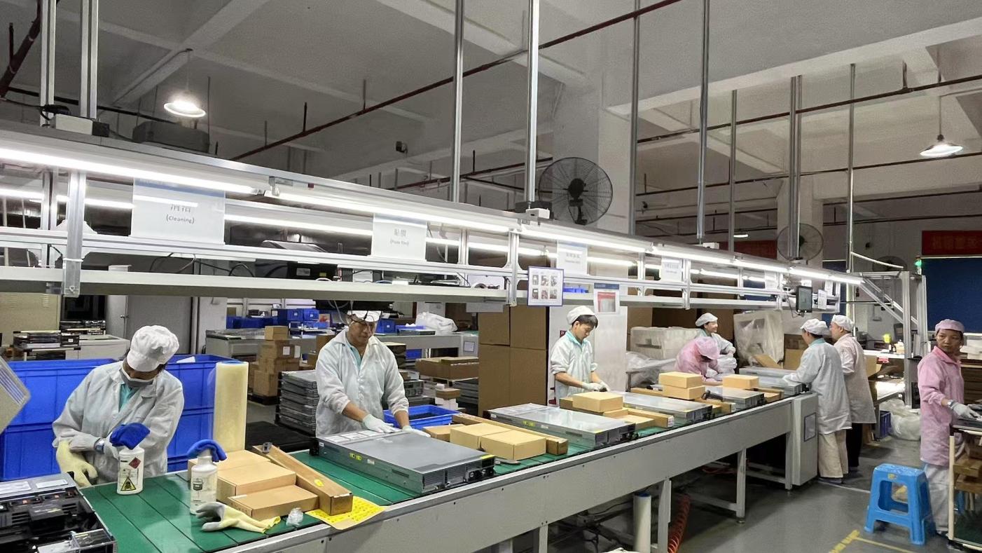
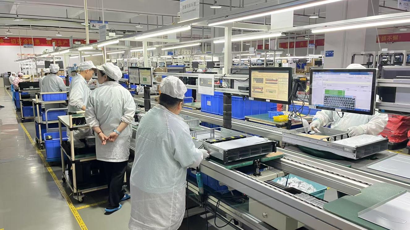
Leveraging our extensive background in memory architecture, high-frequency design runs parallel with our automated assembly capabilities. Our facility features advanced high-precision SMT placement lines and reflow machinery optimized to handle thin, thermally sensitive high-frequency substrates. We specialize in custom multi-layer PCB layout optimization, offering services including:
Over our years of export operations, Celtrix has developed key logistics and engineering support channels spanning over 50 countries. Our target markets include North America, Europe, Southeast Asia, South America, the Middle East, and Oceania. We collaborate with over 1,180 supply chain partners, brand owners, systems integrators, and distributors to ensure project delivery from initial prototyping to high-volume manufacturing.
High-frequency circuit designs have very tight operational tolerances; even minor deviations in trace widths or dielectric thickness can lead to signal loss. Celtrix maintains a strict multi-phase quality control framework to guarantee stable performance.
Our quality assurance workflow runs in accordance with ISO 9001 quality management guidelines. Run by a dedicated team of 56 quality control professionals, every manufacturing run is subjected to rigorous diagnostics, including:
To ensure long-term reliability in harsh environments, we run aging and environmental stress tests on random sample batches, including:
As system architectures transition to higher frequencies, Celtrix is actively preparing for future technologies. Our technology roadmap aligns with emerging international standards for next-generation telecommunications and processing systems.
Next-generation optical transport networks and AI server architectures require trace designs capable of supporting 112Gbps and 224Gbps PAM4 signaling. To achieve these speeds without excessive insertion loss, we are transitioning from standard hybrid stack-ups to ultra-low-loss dielectric structures (e.g., Megtron 8, Rogers RO4000 series with low-profile copper foils). Our fabrication lines are optimized to minimize conductor roughness, copper-weave skew effects, and via reflection anomalies.
Find technical answers below regarding design guidelines, material selection, and manufacturing considerations for high-frequency circuit boards.
High-Frequency PCBs are designed to carry high-frequency RF signals (typically above 1 GHz to over 100 GHz) with minimal signal loss and phase distortion. While standard FR-4 boards have a dissipation factor (Df) around 0.015 to 0.02 at 1 GHz, high-frequency laminates (like Rogers or PTFE) maintain a Df below 0.002, significantly reducing dielectric attenuation and preserving signal integrity.
Hybrid lamination combines high-frequency materials (PTFE, ceramic-filled hydrocarbon) with standard FR-4 layers. This approach is highly cost-effective; high-frequency laminates are placed only on critical RF or high-speed routing layers, while the remaining structural and lower-speed signal layers use standard FR-4. This reduces overall production costs while maintaining high-frequency performance where needed.
At high frequencies, the skin effect concentrates electromagnetic energy near the surface of the conductor. If the copper foil surface is rough, the signal's path is extended, increasing resistive losses. Using Very Low Profile (VLP) or Rolled Annealed (RA) copper foil minimizes this effect, reducing overall insertion loss.
Electroless Nickel Immersion Gold (ENIG) is commonly used, but the nickel layer can introduce signal loss at frequencies above 10 GHz due to its magnetic properties. For higher frequencies, Electroless Nickel Electroless Palladium Immersion Gold (ENEPIG) or Immersion Silver (ImAg) are preferred to minimize loss at the interface.
We use precise etching processes and in-line AOI inspection to monitor trace width variations. Our QA team uses Time Domain Reflectometers (TDR) and Vector Network Analyzers (VNA) to measure impedance profiles on coupon test strips, ensuring that final impedance meets specified tolerances (typically ±10%, down to ±5% on request).
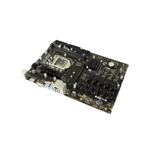
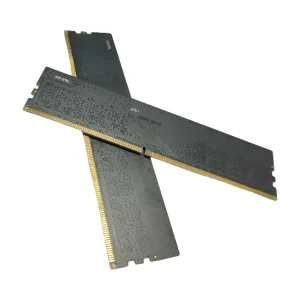
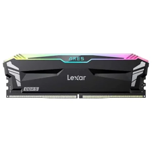
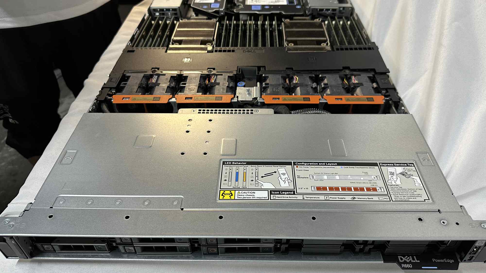
Explore our collection of motherboards, computing RAM modules, and custom PCBA electronic solutions.
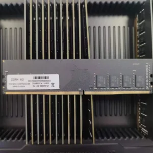
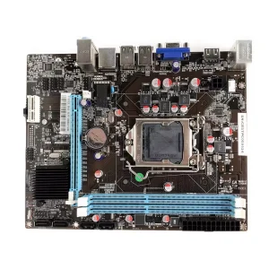
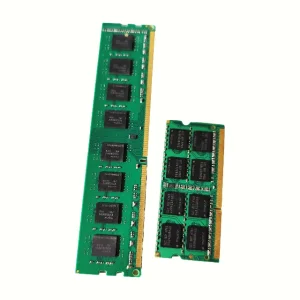
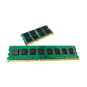
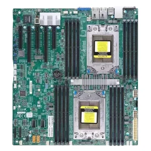
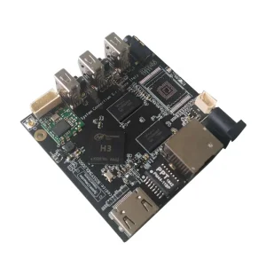
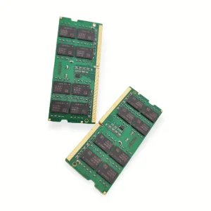
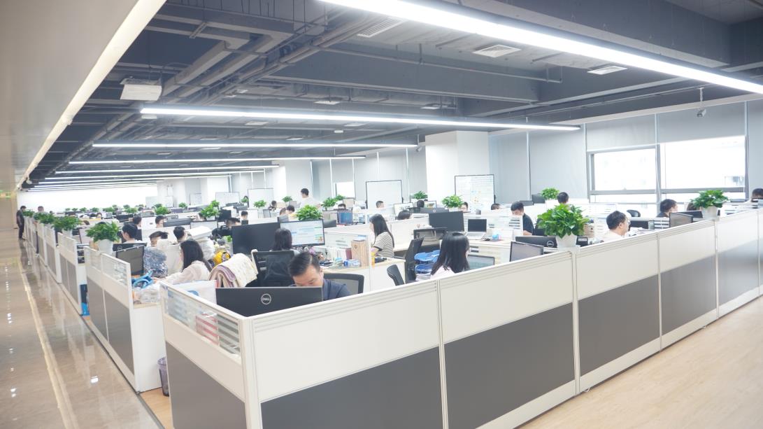
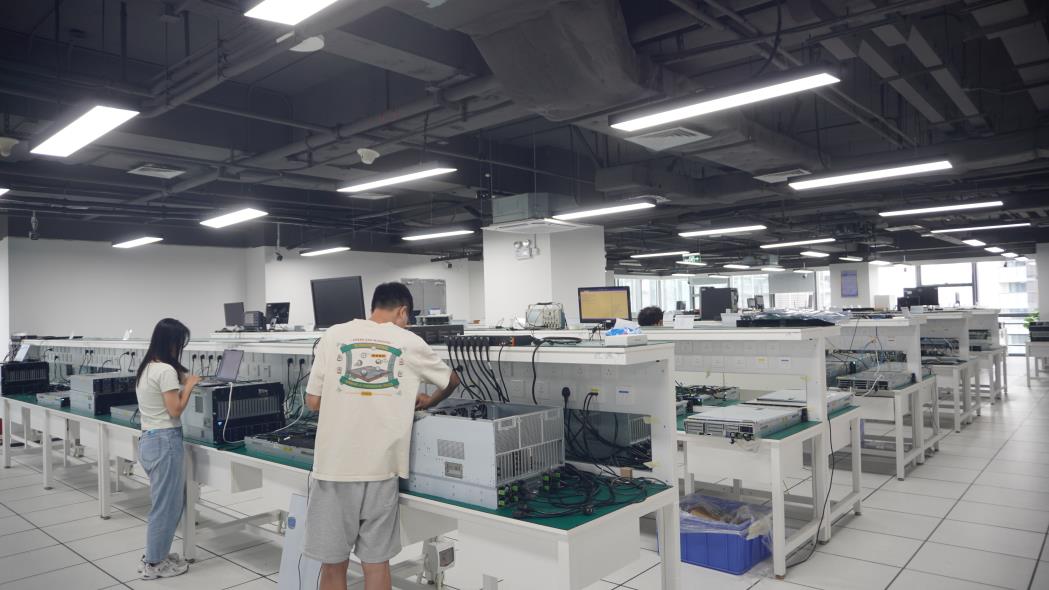
An inside look at our manufacturing facilities, featuring automated high-speed mounting lines, high-precision inspection stations, and our cleanroom SMT assembly floors.
 Celtrix Memory