Celtrix Memory

Engineering Advanced Multilayer PCBs: Foundations of High-Speed Circuitry
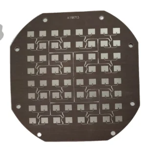
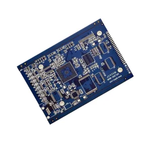
In the modern era of computing, data transmission rates, signal integrity, and thermal management are paramount. As systems compress, the physical constraints of electrical pathways demand highly engineered solutions. Multilayer Printed Circuit Boards (PCBs) act as the structural and electrical backbone of high-frequency devices, routing dense pathways through thin, stacked layers. Unlike single- or double-sided boards, multilayer designs allow engineers to optimize signal shielding, control characteristic impedance, and minimize crosstalk through integrated ground and power planes.
Our manufacturing processes leverage advanced materials and processes to construct boards from 4 to 32+ layers. These materials range from standard High-Tg FR-4 for robust consumer electronics to specialized, high-frequency laminates such as Rogers, Taconic, and Panasonic Megtron families. Precision control over parameters like dielectric constant ($D_k$) and dissipation factor ($D_f$) ensures signal propagation with minimal loss, even at speeds pushing past 32 Gbps.
Understanding HDI (High-Density Interconnect) and Via Structure
As silicon packaging pitches shrink down to 0.4 mm or lower, conventional through-hole routing becomes physically impossible without causing routing blockages. This is where High-Density Interconnect (HDI) technology becomes critical. HDI uses microvias (typically laser-drilled down to 3-4 mils), stacked or staggered via configurations, and buried/blind via paths.
- Blind Vias: Connect an outer layer to at least one inner layer without penetrating the entire board.
- Buried Vias: Connect inner layers together, remaining invisible to the outer surfaces, maximizing surface area availability for component placement.
- Microvias (Laser-Drilled): Extremely small connection vias used specifically in fine-pitch BGA breakouts, typically filled with electroplated copper for maximum conductivity.
The Strategic Advantage of China's PCB & PCBA Ecosystem
Procuring multilayer PCBs and full-scale SMT PCBA (Surface Mount Technology Printed Circuit Board Assemblies) from a specialized Chinese partner offers massive advantages. China's Pearl River Delta and Yangtze River Delta regions host the world's most dense supply chain networks for raw materials, copper-clad laminates (CCL), chemical processors, and electronic component distributors.
This industrial concentration translates directly to:
- Unparalleled Supply Chain Agility: We source custom laminates, specific solder masks, and specialized finishes (such as Immersion Gold, Immersion Silver, OSP, or HASL) within days rather than weeks.
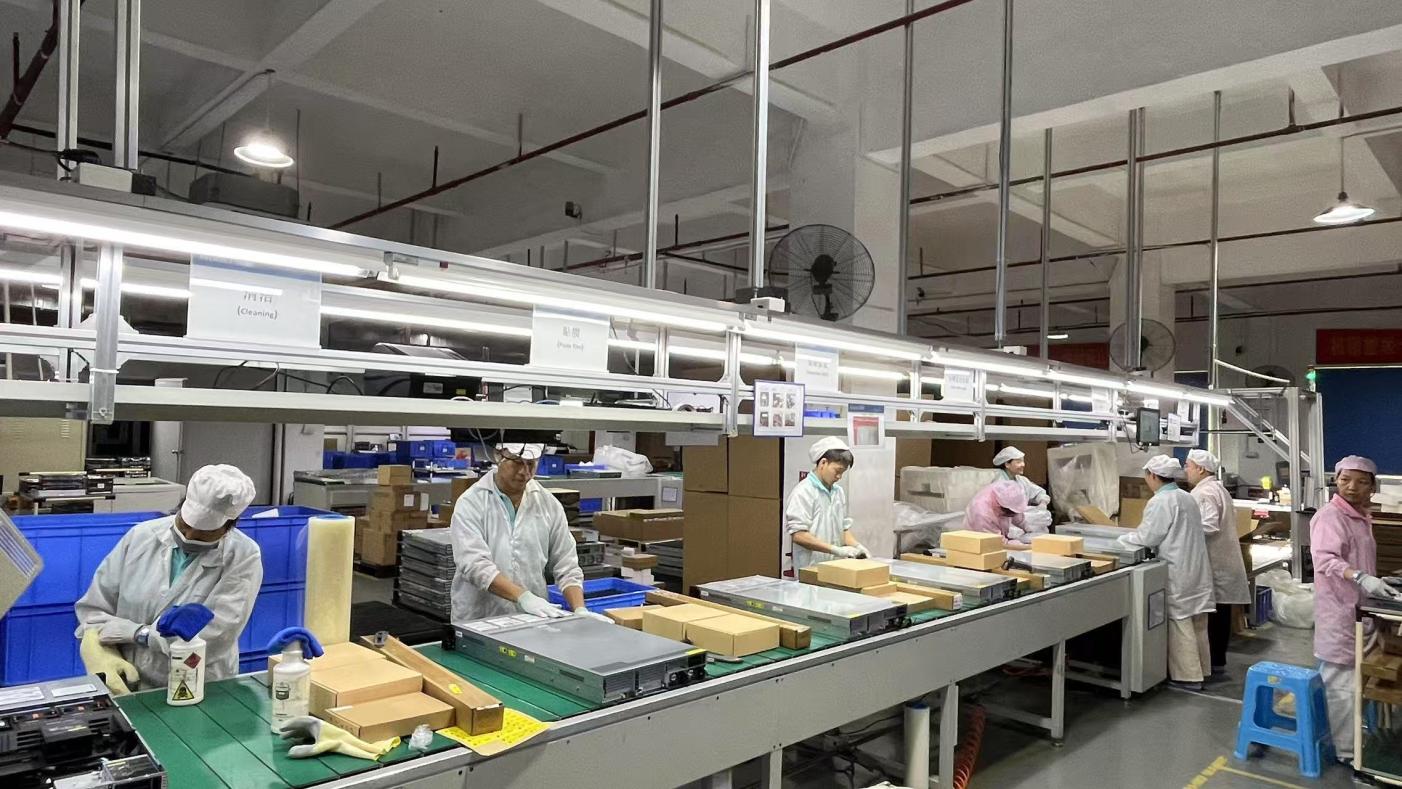
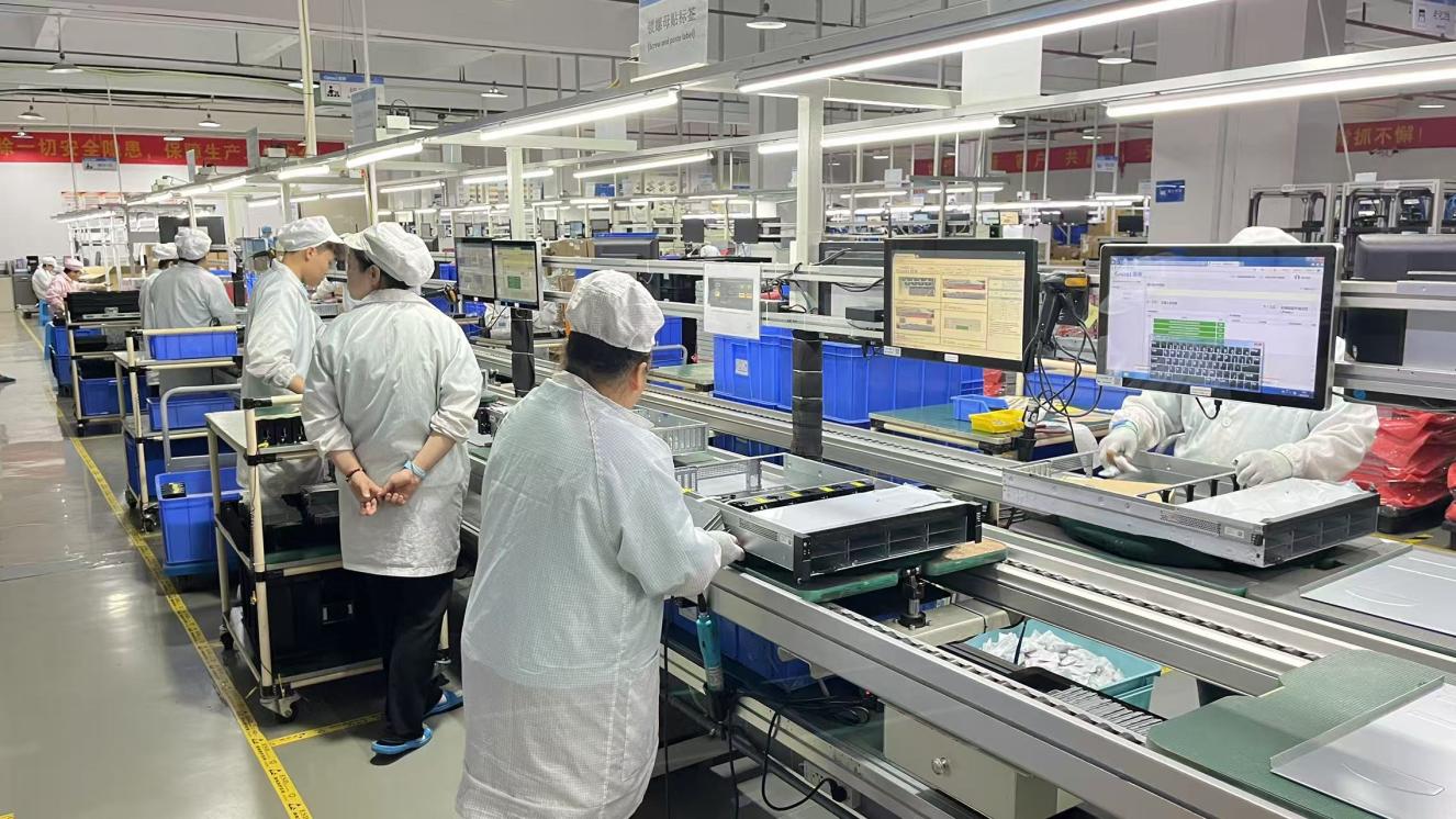
- Highly Scalable Production: Our 28,600 m² factory in China is optimized for both fast-turn prototyping (under 24-48 hours for standard stack-ups) and high-volume mass production.
- Advanced SMT Automation: By combining high-speed pick-and-place equipment, automated optical inspection (AOI), 3D X-ray systems, and in-line testing, we maintain high yields and low manufacturing defect rates (measured in DPPM).
Global OEM Sourcing & Procurement Requirements
Enterprise procurement teams demand more than just competitive pricing; they require deep operational resilience, certified quality management systems, and transparent manufacturing processes. Modern buyers evaluate suppliers on the following core metrics:
- DFM (Design for Manufacturability) Review: Analyzing layouts prior to manufacturing to eliminate layout errors, trace-to-edge issues, and solder masking violations.
- Quality Traceability: Complete inspection logs of raw materials, solder quality, assembly parameters, and functional tests (FCT).
- Compliance Standards: Conformity with IPC Class 2/3 regulations, UL 94V-0 flammability ratings, RoHS environmental compliance, and ISO 9001:2015 frameworks.
Industry Macro-Solutions: Where High-Precision PCBs Excel
1. High-Performance Computing (HPC) & Servers
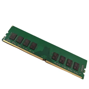
With the rapid adoption of AI training networks, servers require ultra-high speed DDR5 memory channels and PCIe Gen 5/6 routing. We engineer PCBs with up to 24 layers featuring controlled impedance margins below ±5%. Utilizing low-loss materials reduces attenuation over long traces, supporting multi-gigahertz operations.
2. Automotive Electronics & Advanced Driver Assistance Systems (ADAS)
Automotive designs prioritize safety and longevity. Heavy copper layers (up to 4 oz or more) are utilized for high-power distribution, while thermal management via copper coins or filled thermal vias guarantees stable operation in extreme engine bay conditions.
3. Industrial Automation & Instrumentation
Industrial control circuits operate in hostile environments filled with electromagnetic interference (EMI). Incorporating dedicated shield layers, galvanic isolation zones, and heavy gold plating guarantees reliable system operation inside automated plants.