Celtrix Memory
1 / 5
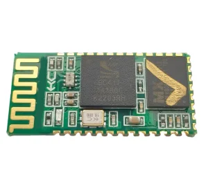
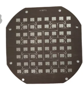
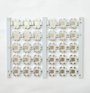
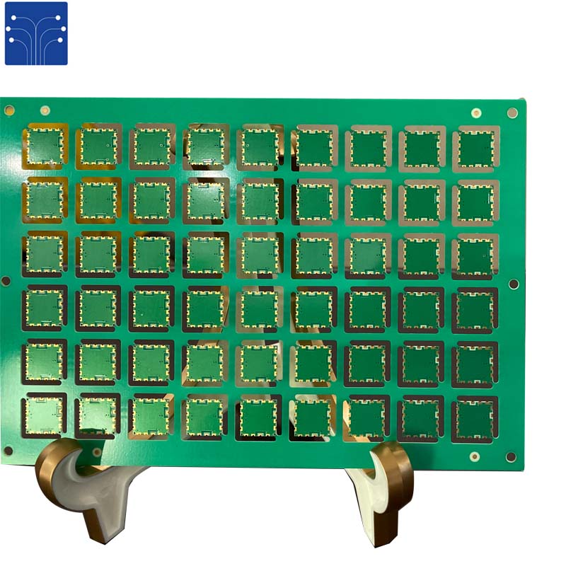
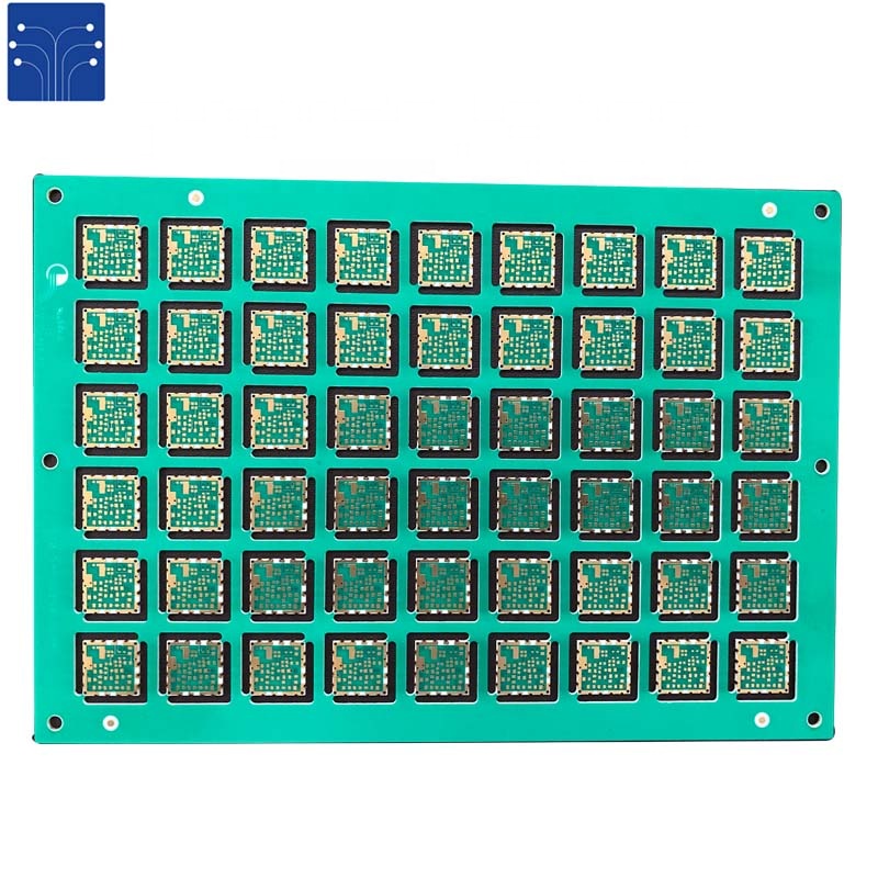
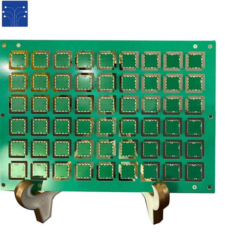
We have invested in the best equipment, environment, and staff training. We have a production capability for standard and HDI, Rigid, RF, and high-frequency PCBs, together with through-hole and minimum 0201 chips, 0.2mm pitch BGA balls SMD soldering, available in small batch, mid-volume, and high-volume quantities.
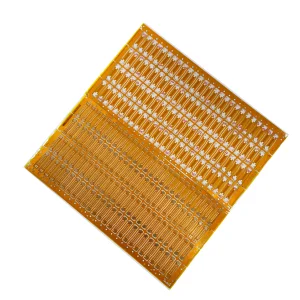
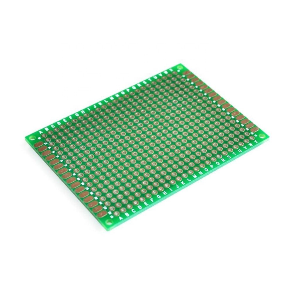
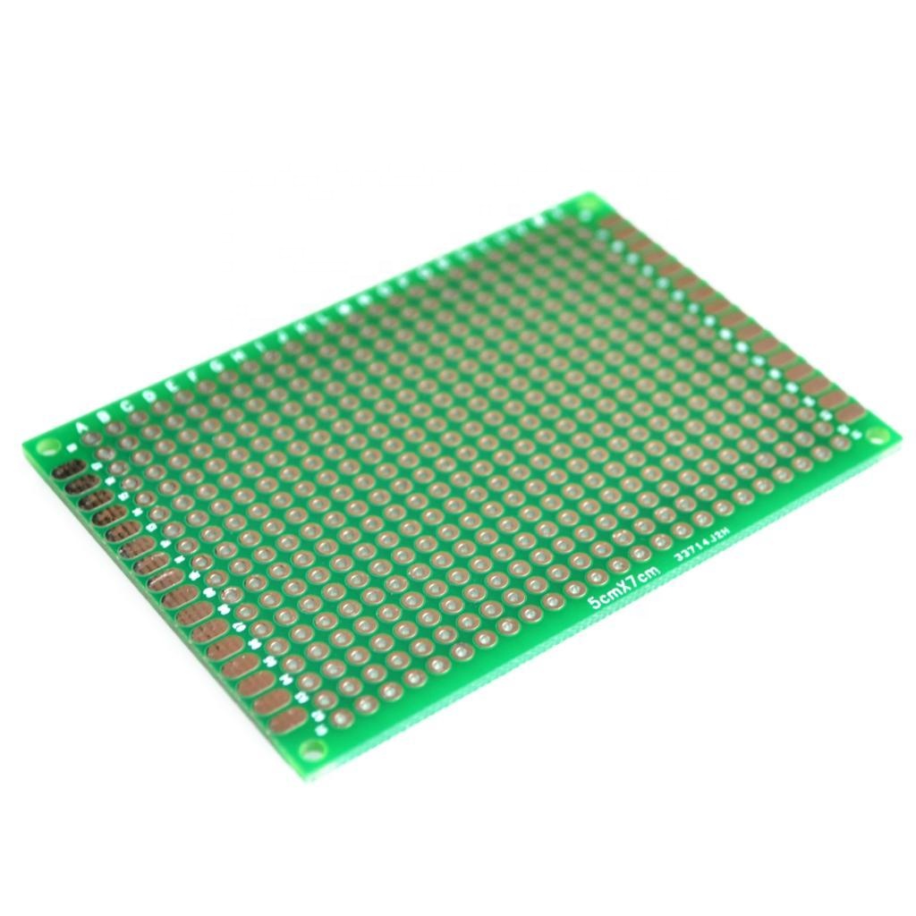
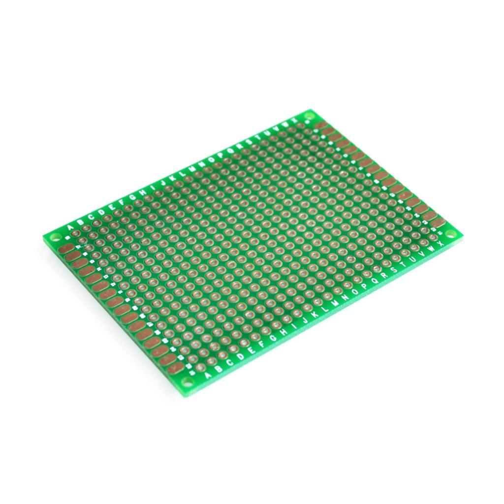
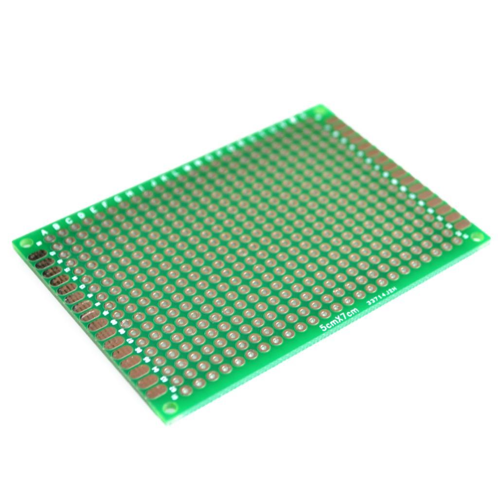
7x9cm, 9x15cm, Pack of 4, each size 2 pieces. The boards are thick and double-sided. Material: FR4 glass fiber. Solders well, and both sides can be scored cleanly. No sharp edges, highly manageable, sturdy, and easy to use. The plated holes are pre-tinned and very solid. Each column and row is clearly labeled to make assembly less error-prone. PCB boards are excellent for migrating your circuit from a breadboard to a permanent circuit board, making them suitable for DIY projects and electronic designing.
Printed Circuit Board Tinned Universal PCB Circuit Board in green. We are glad to send free samples to you; you only need to cover the shipping cost.
| Items | Capacity |
|---|---|
| 1. Base Material | FR4 glass fiber |
| 2. Copper Thickness | 1oz copper |
| 3. Technics Characteristic | Normal |
| 4. Technical Requirement | Normal |
| 5. Standard Produce Time | 7-10 days |
| 6. Fast Produce Time | 24h ~ 72h |
| Customer Service | We provide professional pre-sales and after-sales service, and we will try our best to assist you with any product inquiries. |
| Product Warranty | 100% quality warranty. If you experience any issues or are not satisfied with the products, we offer an unconditional refund policy. |
We have established a quality system aligned with ISO9001 and strictly implement the IPC Class III standard to inspect overall quality. 100% inspection includes electrical testing and AOI inspection. We carry out high-voltage tests, impedance tests, microsections, solderability tests, and other professional evaluations to keep pace with the demands of high-tech products.
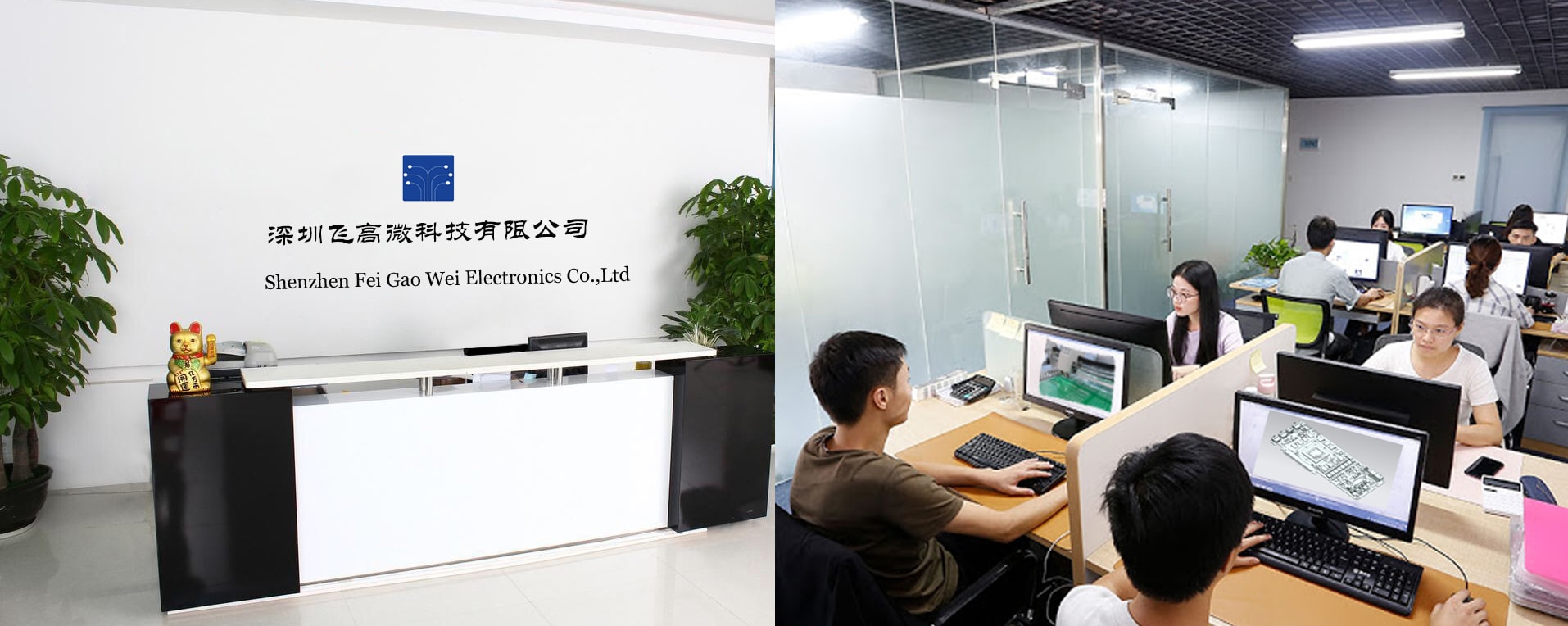
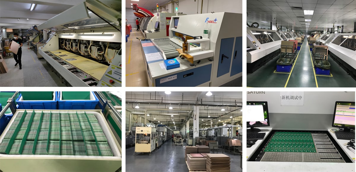
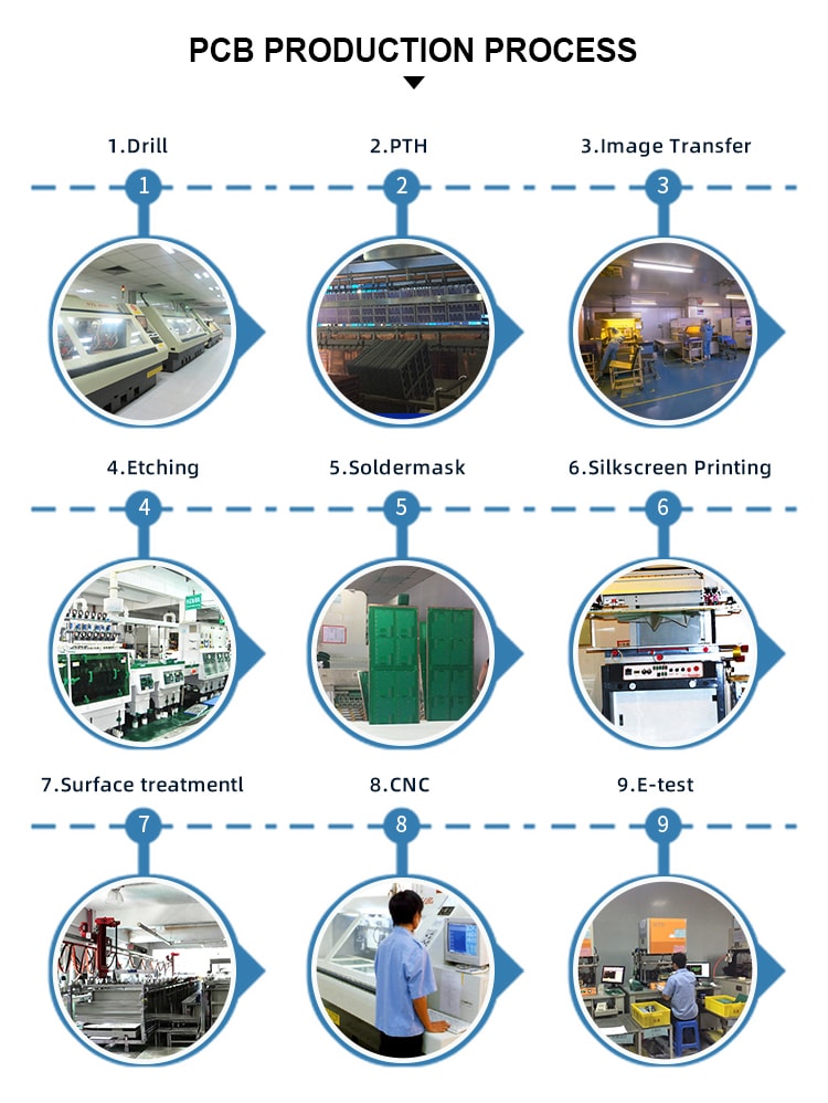
We have been manufacturing printed circuit boards for more than 20 years. Established in 1990, we act as a competitive, high-tolerance, high-quality PCB supplier for small to medium-volume production runs. Whether you require a prototype printed circuit board assembly or large-volume PCB production, we possess the capacity and technical knowledge to satisfy your requirements.
We pride ourselves on offering professional service with a collaborative approach where quality remains of paramount importance, in accordance with our ISO9001 Quality Management system and UL Approval.
We specialize in Quick-turn PCB services, achieving turnaround times as fast as 24 hours. When your project demands fast and rapid PCB prototyping, you can count on us to deliver high-quality printed circuit boards on time and at competitive prices.
We encourage all prospective clients to visit our facilities. We maintain an open-door policy for all customers, both new and old. Once you observe our operations and consult with our expert staff, you can be assured of our ability to meet your individual production needs.
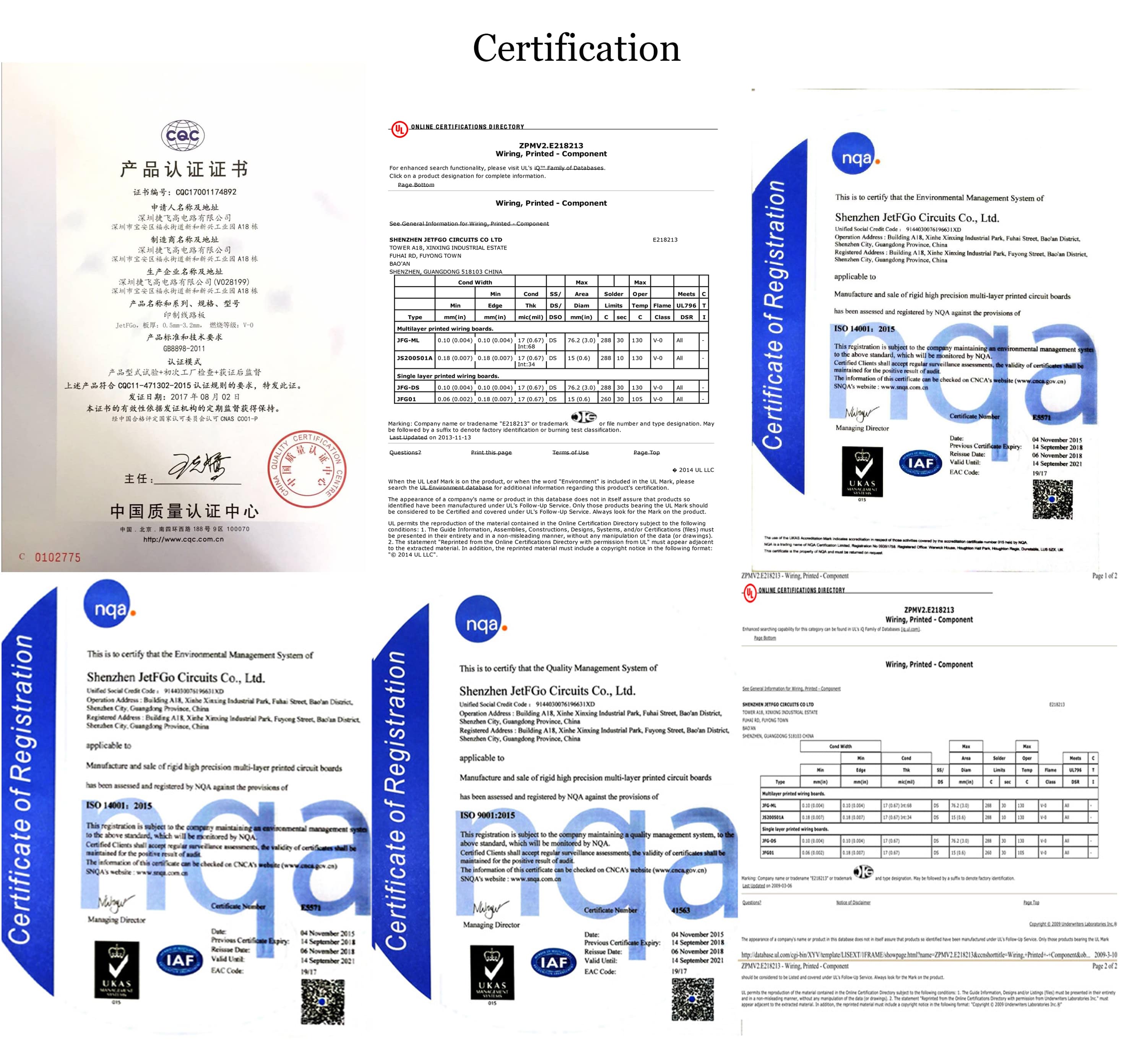
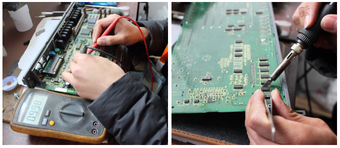
We have over 15 professional engineers, and all products are fully tested before warehousing and shipping.
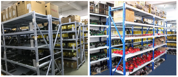
We maintain a large stock of products to ensure quick response and reliable support for all client requests.
We focus not only on providing quality products but also on offering safe and secure packaging. We provide structured packaging options for all shipments:
Outer cartons can be custom-printed with customer markings, addresses, and destination information as specified.
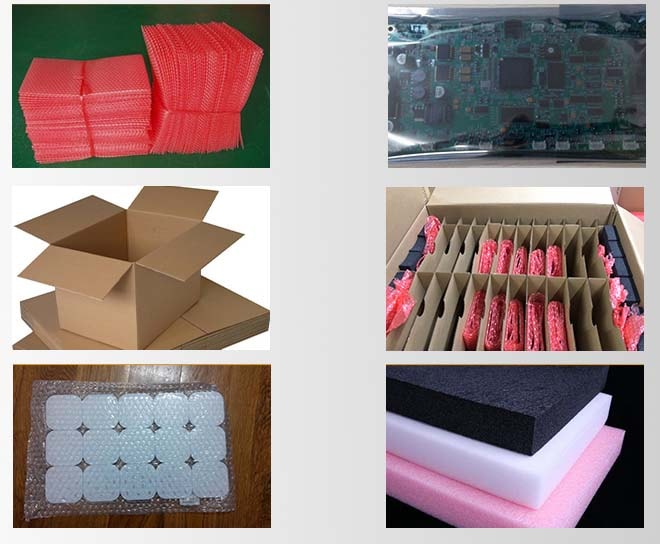

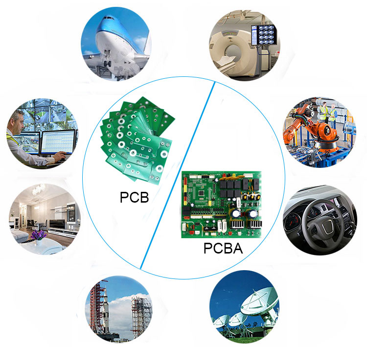
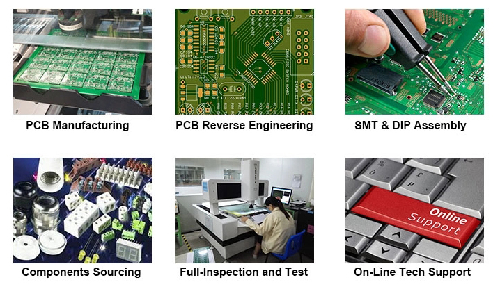
We provide one-stop PCB/PCBA customization services to meet all customer specifications.
To ensure the quality of outgoing PCB/PCBA units, we perform comprehensive quality testing before shipment:
We offer a 3-month warranty for used parts and a 1-year warranty for new parts. If parts fail to operate properly upon receipt, they can be returned to us within 7 days.
We typically use 3cm thick foam board lining within the box to secure and protect all parts. Sturdy cartons are used standard, and customized wooden boxes can be constructed for heavy shipments.
Yes, we use precise testing equipment to ensure all parts are 100% functional before shipment. Since we maintain substantial stock, shipping typically takes 1-2 business days.
Yes, we can copy the design directly from your physical sample to generate Gerber files, which are then used for production. We can also generate Gerber files from schematic diagrams provided by the customer.
Yes, panelization of multiple part numbers is common practice at our facility. This helps reduce setup costs and overall assembly expenses for the customer.
All customer design files are kept confidential and protected within our factory. We do not share design data with third parties and are ready to execute standard Non-Disclosure Agreements (NDAs).