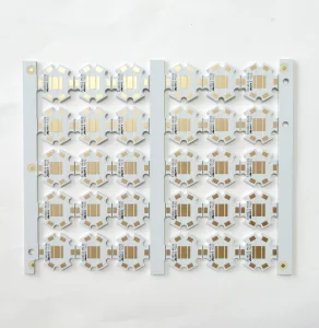
Explore our specialized prototype layouts engineered for quick deployment and reliable thermal dissipation in harsh environmental conditions.


The Australian electronic engineering sector is undergoing a profound paradigm shift. Driven by federal mandates to secure domestic tech pipelines and accelerate sovereign manufacturing capability, key sectors such as defence aerospace, mining technology, agritech, and medical systems are demanding high-speed, high-density multilayer PCBs.
Australia's geographic expanse and decentralized layout require hardware products that can operate reliably under harsh physical environments. Whether it is a seismic monitoring device in the Western Australian desert or telemetry equipment in Queensland mines, the physical integrity of a multi-layer circuit board determines the survival of the system.
While domestic Australian facilities cater effectively to rapid prototyping and low-volume assembly, the high cost of raw laminates, limited domestic supply chains for high-Tg substrates, and high labor rates present clear economic obstacles for commercializing products at scale. Consequently, engineering firms in Sydney, Melbourne, Brisbane, and Adelaide are adopting hybrid supply models. They execute critical R&D phases onshore and coordinate with advanced offshore manufacturers like Celtrix Memory Technologies to manage medium-to-high volume production. This approach secures E-E-A-T (Expertise, Experience, Authoritativeness, and Trustworthiness) standards while optimizing production costs.
As modern data architectures transition to PCIe Gen 5 and Gen 6 interfaces, signal preservation on multi-layer PCBs has become a critical design priority. Standard FR-4 laminates are no longer sufficient for these operating frequencies due to high dielectric losses.
We work with high-frequency laminates including Rogers (RO4350B, RO4003C), Taconic (TLY-5), and high-Tg FR-4 (Shengyi S1170, Isola 370HR) to limit dielectric loss and control CTE (Coefficient of Thermal Expansion) mismatch across layers.
We execute strict trace-width validation and differential pair calculations with tolerances within ±5%. Using TDR (Time Domain Reflectometry) testing, we ensure clean transmission paths for high-speed differential signal pairs.
Supporting advanced HDI layouts with blind vias, buried vias, microvias (laser drilled down to 0.1mm), and VIPPO (Via In Pad Plated Over) processes to maximize space and lower parasitic capacitance.
Our factory processes multilayer designs up to 32 layers with minimum line widths and spacings down to 3 mil (0.075 mm). These capabilities enable us to integrate high-density components, including BGA packages with pitches down to 0.4 mm, which are increasingly common in modern IoT edge nodes and industrial computing platforms.
Industrial sectors in Australia present unique operating challenges, requiring dedicated structural engineering for electronic components. Our technical teams align manufacturing parameters with the specific demands of each sector:
Building a reliable supply chain requires a strong commitment to quality and regulatory standards. For Australian electronic designers, regulatory compliance is key to entering domestic and global markets:
Every product manufactured by Celtrix aligns with international standards, including ISO 9001:2015, ISO 14001, and UL94V-0 certification. For safety-critical industries, we support development pathways adhering to AS9100 standards for aerospace and defense, and ISO 13485 for medical technology.
All production processes comply with RoHS and REACH requirements, facilitating hassle-free importation into Australia. Our team provides full traceability documentation, chemical safety datasheets, and physical test reports with every shipment.
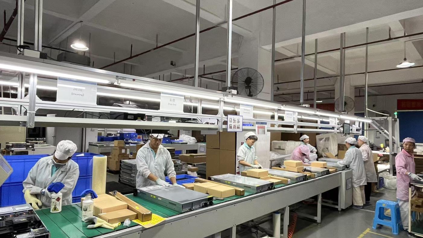
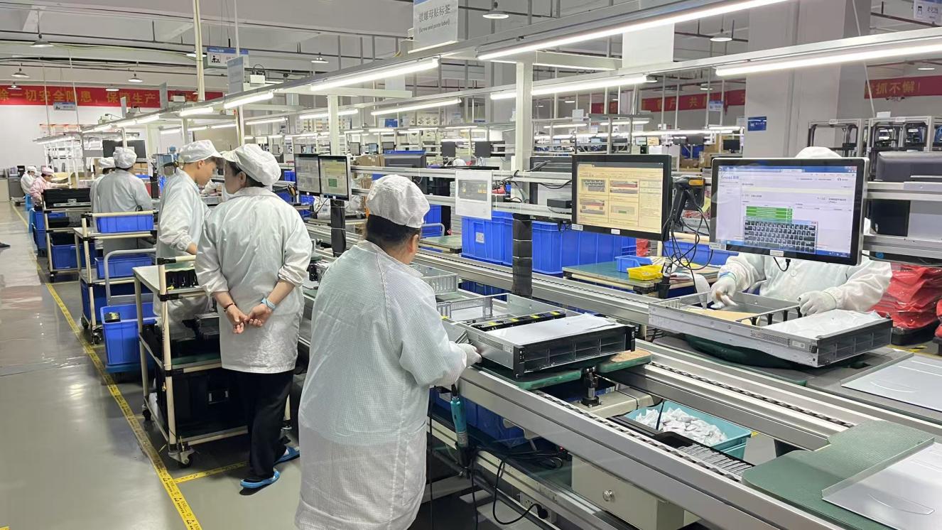
Operating from our 28,600 m² smart factory in Shenzhen, Celtrix incorporates automation at every stage of the manufacturing process. Our facility integrates automated material handling systems, high-speed SMT placement lines, and inline inspection systems. This level of automation reduces human error, increases yield, and ensures consistent quality.
We mitigate global component shortages through long-term partnerships with leading component distributors, including Arrow, Avnet, and Future Electronics. Our central warehouse keeps a large buffer stock of standard passive components, microcontrollers, and high-performance memory ICs, allowing us to reduce lead times for turn-key PCBA projects.
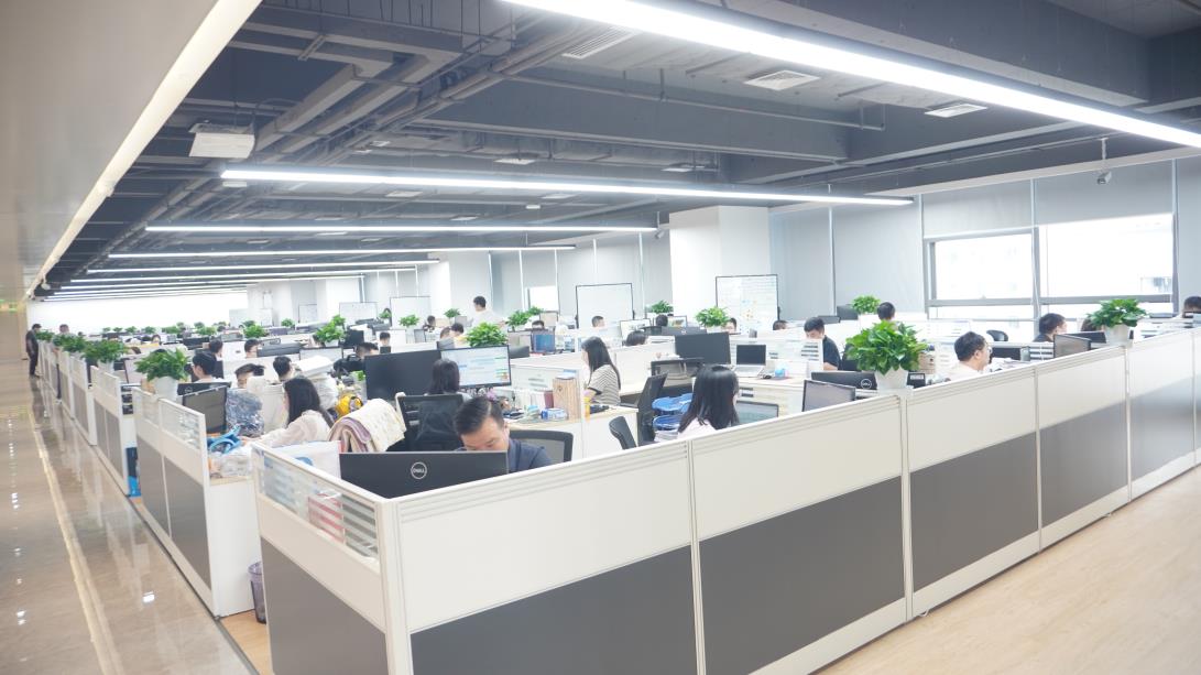
With an experienced engineering team (consisting of 142 R&D engineers), we provide quick DFM feedback. This helps design engineers fix potential manufacturing issues—such as component clearance conflicts or thermal imbalances—before production starts.
Common questions regarding technical capabilities, logistics, compliance, and custom ordering for Australian projects.
For standard prototype builds (2-6 layers), our manufacturing cycle takes 3-5 business days. Once shipped via air express (DHL/FedEx), packages generally arrive in Sydney, Melbourne, or Brisbane within 3-4 business days. For mass production runs (8+ layers), shipping times vary between 10-15 business days depending on design complexity.
While the final C-Tick/RCM compliance certification is obtained by the Australian importer, we design and manufacture PCBs to pass rigorous EMI/EMC testing. We perform controlled impedance testing and advise on optimal copper grounding structures to minimize electromagnetic interference.
Yes, we work with specialized high-frequency laminates, including Rogers (RO4350B, RO4003C) and Taconic (TLY-5). We keep standard stock of these materials for high-frequency RF systems, radar designs, and communication projects.
Yes, we offer complete turn-key PCBA services. This includes PCB fabrication, component sourcing, SMT placement, manual assembly for complex connectors, programming, and functional testing.
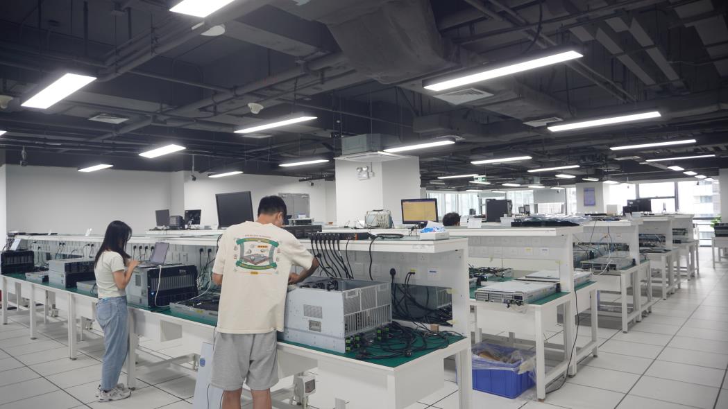
Our Quality Control division runs inline inspections for all Class 3 designs. This includes Solder Paste Inspection (SPI), Automated Optical Inspection (AOI) before reflow, 3D X-Ray Inspection (AXI) for BGA packages, Flying Probe testing, and final visual inspection by IPC-certified quality engineers.
Review our standard and custom-tailored assembly solutions, memory modules, and specialized electronics for industrial computing architectures.
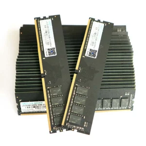
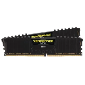
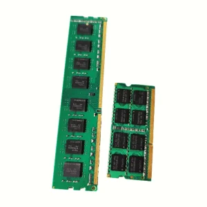
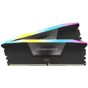
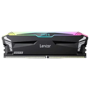
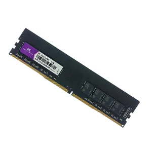
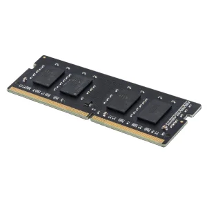
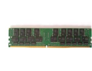
Celtrix Memory Technologies Co., Ltd. is a dedicated developer and manufacturer of high-performance DRAM solutions and precision SMT/PCB systems. Established in 2017, we operate a modern 28,600 m² factory designed to produce reliable computing modules for consumer, industrial, and enterprise applications.
With 9 years of industry experience and 7 years of export history, we serve system integrators, distributors, and OEM/ODM clients in over 50 countries. Our operations are backed by 142 R&D engineers and 56 Quality Assurance professionals to ensure all products align with global specifications.
Factory Address & Main Markets:
Providing advanced electronic assemblies for key global regions including North America, Europe, Southeast Asia, South America, the Middle East, and Oceania.
 Celtrix Memory